Lower electrode assembly and chemical vapor deposition equipment comprising the same

A technology of chemical vapor deposition and electrode assembly, which is applied in the field of microelectronics, can solve the problems of the temperature uniformity of the carrier board, the loss of heating efficiency, and the very high requirements for the material of the carrier board, so as to improve the heating efficiency and heat utilization rate and reduce the cost. Effect

Inactive Publication Date: 2013-06-19
BEIJING NAURA MICROELECTRONICS EQUIP CO LTD
View PDF4 Cites 4 Cited by
  • Summary
  • Abstract
  • Description
  • Claims
  • Application Information

AI Technical Summary

Problems solved by technology

[0005] 1. The temperature uniformity of the carrier board needs to be improved
2. The carrier board in the above-mentioned PECVD equipment needs to be grounded, so the requirements for the material of the carrier board are very high, which leads to an increase in the cost of the carrier board
At the same time, due to the very large area of ​​the carrier board, the grounding effect of the carrier board is not good
3. In the above PECVD equipment, only the carrier plate can be raised and lowered, resulting in a serious loss of heating efficiency

Method used


Image

  • Lower electrode assembly and chemical vapor deposition equipment comprising the same
  • Lower electrode assembly and chemical vapor deposition equipment comprising the same
  • Lower electrode assembly and chemical vapor deposition equipment comprising the same

Examples


Embodiment Construction

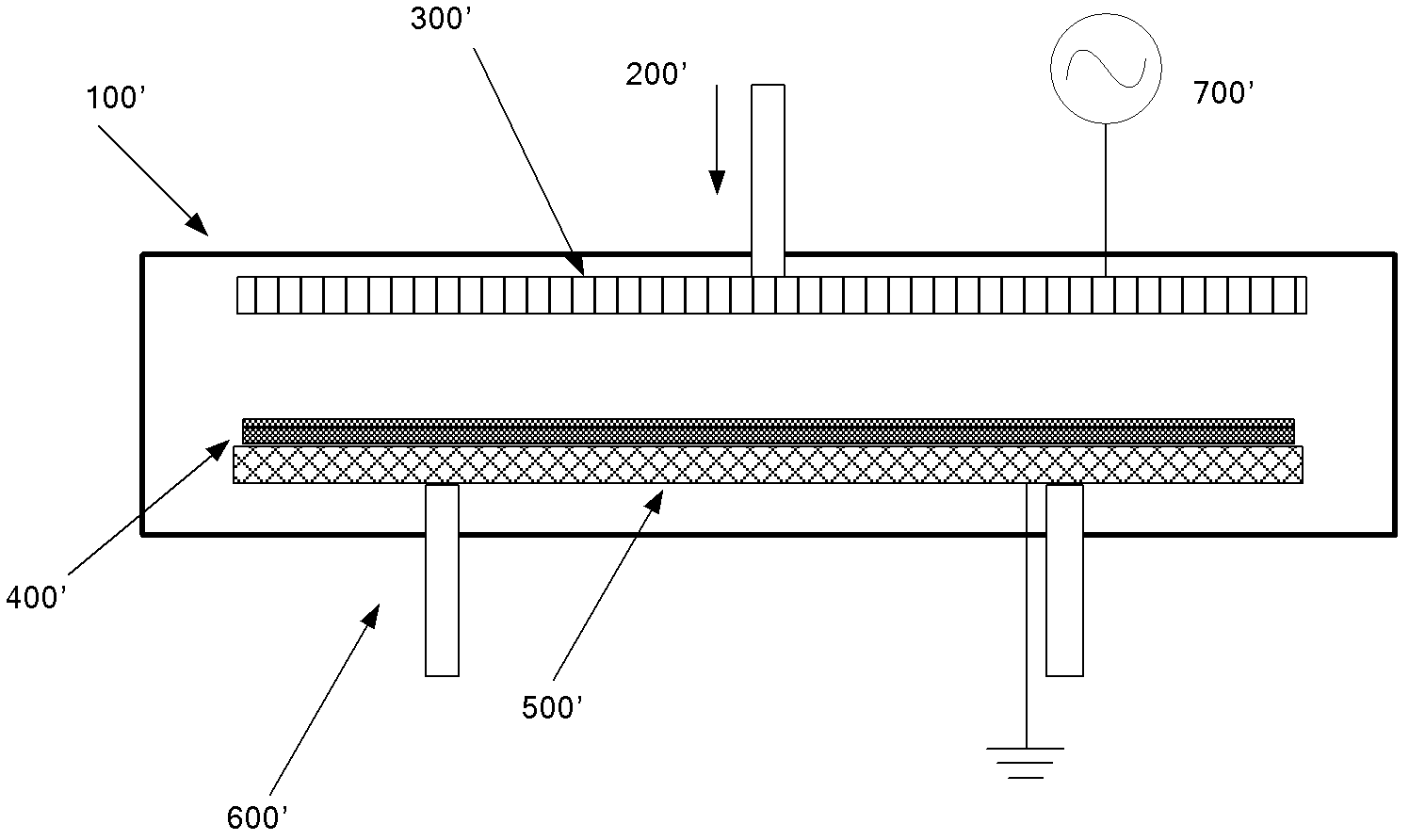
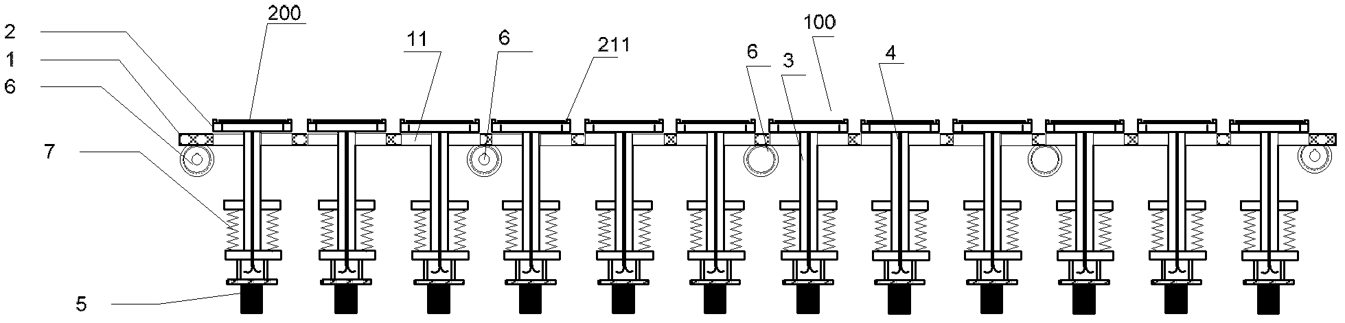
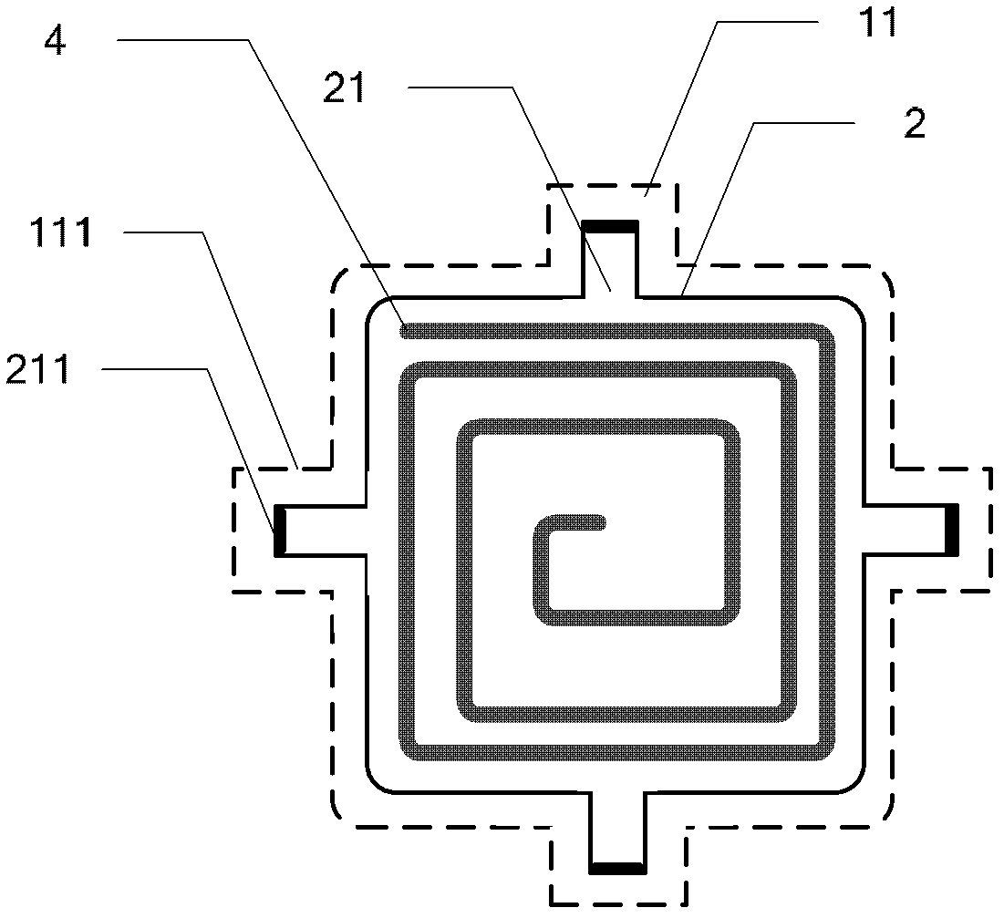
[0040] Embodiments of the present invention are described in detail below, examples of which are shown in the drawings, wherein the same or similar reference numerals designate the same or similar elements or elements having the same or similar functions throughout. The embodiments described below by referring to the figures are exemplary only for explaining the present invention and should not be construed as limiting the present invention.

[0041] In describing the present invention, it should be understood that the terms "center", "longitudinal", "transverse", "length", "width", "thickness", "upper", "lower", "front", " The orientation or positional relationship indicated by "rear", "left", "right", "vertical", "horizontal", "top", "bottom", "inner" and "outer" are based on the orientation or position shown in the drawings The positional relationship is only for the convenience of describing the present invention and simplifying the description, but does not indicate or im...


PUM


Abstract

The invention provides a lower electrode assembly and semiconductor processing equipment comprising the lower electrode assembly. The lower electrode assembly comprises a substrate, a tray, a tray support, a heater and a lifting mechanism, wherein the substrate is used for conveying and carrying a wafer; the tray support is connected with the tray to support the tray; the heater is arranged in the tray; and the lifting mechanism is connected with the tray support and used for lifting and descending the tray so that the heater can better heat the wafer. According to the lower electrode assembly, the heating efficiency and the heat utilization rate are improved, and cost is lowered.

Description

technical field [0001] The invention relates to the technical field of microelectronics, in particular to a lower electrode assembly and chemical vapor deposition equipment with it. Background technique [0002] PECVD (Plasma Enhanced Chemical Vapor Deposition) equipment places wafers on a flat carrier. And the carrier is grounded, and the upper electrode is connected to intermediate frequency or radio frequency, so as to form a plasma between the upper electrode and the carrier to deposit and generate a film layer on the wafer. [0003] figure 1 It is a structural diagram of a flat-plate PECVD equipment, which includes a reaction chamber 100' with a reaction chamber, an air inlet 200', an upper electrode plate 300' and a carrier plate 400' arranged in the reaction chamber 100' , and the lifting cylinder 600' and the heating chamber 500' that control the lifting of the carrier. Wherein, the upper electrode plate 300' is connected to the radio frequency source 700', and th...

Claims


Application Information

Patent Timeline
IPC IPC(8): C23C16/50
Inventor 袁强
Owner BEIJING NAURA MICROELECTRONICS EQUIP CO LTD
Why Eureka
Try Eureka