Gate-oxide etching method and multi-grid-electrode manufacturing method

A multi-gate and gate oxide technology, applied in the field of process technology and gate oxide layer etching, can solve serious problems such as image device quality, large particle defects, poly layer snowball effect, etc.

Active Publication Date: 2013-06-19
CSMC TECH FAB2 CO LTD
View PDF9 Cites 6 Cited by
  • Summary
  • Abstract
  • Description
  • Claims
  • Application Information

AI Technical Summary

Problems solved by technology

The wet etching time becomes a key factor to ensure the quality of multi-gate devices: if the etching time is too short, the first gate oxide layer will not be etched clean, and the remaining gate oxide layer will be etched in the second When the gate oxide layer is fabricated, an overlap will be formed, which will cause the gate of the first device to be too high and affect the electrical properties of the device
If the etching time is too long, after the first gate oxide layer is etched, the acidic liquid in the etching solution will further corrode the su...

Method used


Image

  • Gate-oxide etching method and multi-grid-electrode manufacturing method
  • Gate-oxide etching method and multi-grid-electrode manufacturing method
  • Gate-oxide etching method and multi-grid-electrode manufacturing method

Examples


Embodiment Construction

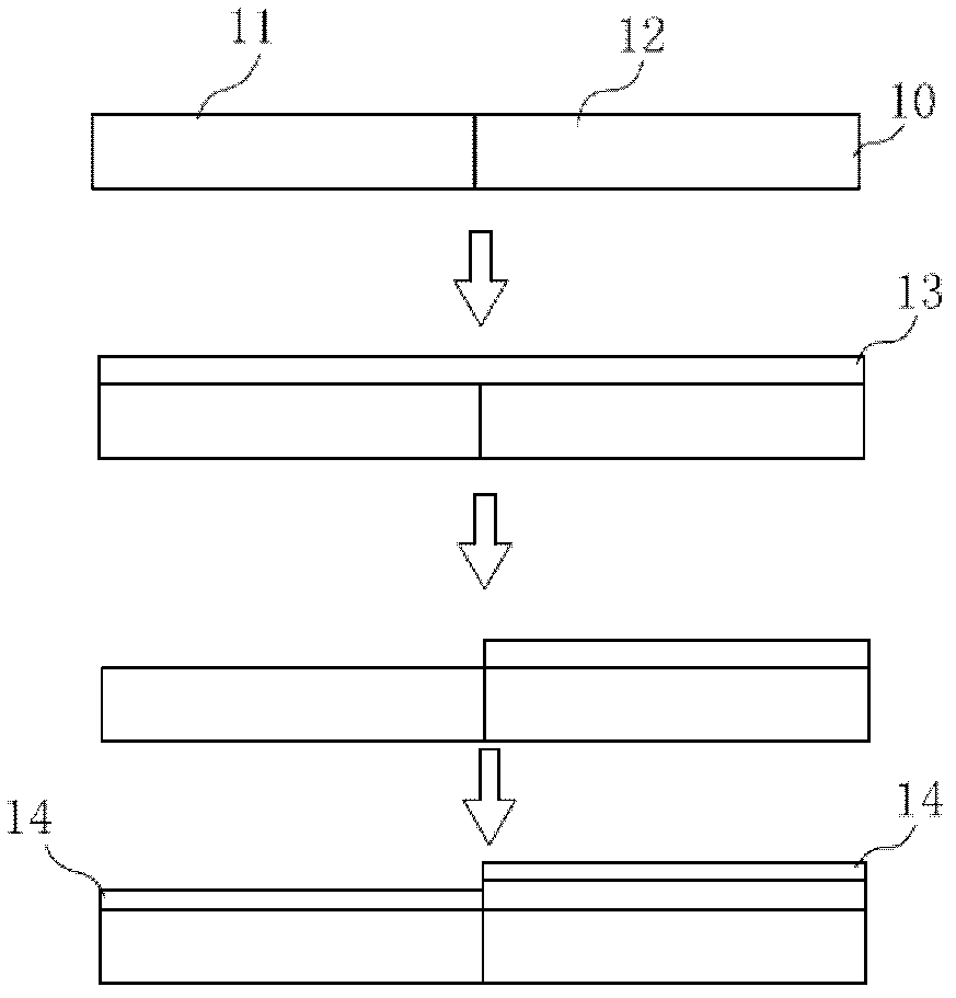
[0042] As mentioned in the background technology, in the fabrication of multi-gate process, due to the need to etch the previous gate oxide layer, and the current etching method is easy to introduce residue defects or large particle defects, resulting in multi-gate device performance is affected.

[0043] In view of this, an etching method for the gate oxide proposed by the present invention can reduce the damage to the substrate surface under the condition of completely etching the gate oxide, thereby reducing the generation of particle defects and making the multi-gate The quality of the pole workmanship has been improved.

[0044] The gate oxide etching method of the present invention will be described in detail below. It should be noted that the gate oxide layer etched by the etching method of the present invention refers to the pre-sequence gate oxide layer used in the multi-gate process. The purpose of etching is to pattern the gate oxide layer so that the surface of th...


PUM


Abstract

The invention provides a gate-oxide etching method and a multi-grid-electrode manufacturing method. The gate-oxide etching method includes controlling over-etching time of buffered oxide etch (BOE), enabling over-etching time of the BOE to be smaller than 30% of main etching time, and matching with concentration ratio of APM. According to the method, damage on surface of a lining can be reduced on the condition that the gate-oxide is completely etched. Meanwhile, the gate-oxide etching method is applied to the multi-grid-electrode manufacturing method, and defects of particulate matters can be reduced, so that quality of multi-grid-electrode components is greatly improved.

Description

technical field [0001] The invention relates to a manufacturing process in the field of semiconductors, in particular to a method for etching a gate oxide layer in the process of manufacturing a multi-gate. Background technique [0002] With the rapid development of semiconductor manufacturing technology, in order to achieve faster computing speed, larger data storage capacity and more functions of semiconductor devices, semiconductor wafers are developing towards higher component density and high integration. In the manufacturing process of some chips, the gate thickness required for these devices is often inconsistent due to the electrical properties of different devices, so a multi-gate manufacturing process has been formed in the industry. [0003] See figure 1 , taking the double gate manufacturing process as an example: define the regions of the first device 11 and the second device 12 on the substrate 10 respectively, first form a layer of gate oxide layer 13 with th...

Claims


Application Information

Patent Timeline
IPC IPC(8): H01L21/311H01L21/28
Inventor 陈亚威
Owner CSMC TECH FAB2 CO LTD
Why Eureka
Try Eureka