
Digital filter, collocation method of digital filter, electronic device and wireless communication system

A digital filter and filter technology, applied in digital technology networks, electrical components, impedance networks, etc., can solve the problems of poor scalability and high cost, and achieve the effects of avoiding material waste, reducing costs, and improving scalability.

Active Publication Date: 2013-06-19
HUAWEI TECH CO LTD
View PDF4 Cites 23 Cited by
  • Summary
  • Abstract
  • Description
  • Claims
  • Application Information

AI Technical Summary

Problems solved by technology

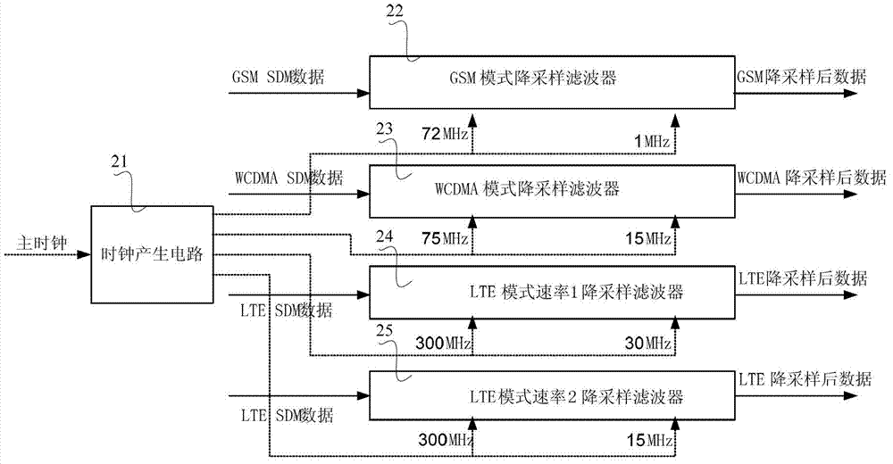
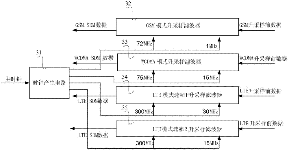
[0022] In view of this, the purpose of the embodiments of the present invention is to provide a digital filter and its configuration method, electronic equipment and a wireless communication system, so as to overcome the problems of digital filters in the prior art during the conversion process of various operating modes. When implementing digital sampling filtering, the problem of excessive cost and poor scalability

Method used


Image

  • Digital filter, collocation method of digital filter, electronic device and wireless communication system
  • Digital filter, collocation method of digital filter, electronic device and wireless communication system
  • Digital filter, collocation method of digital filter, electronic device and wireless communication system

Examples


Embodiment 1

[0084] Such as Figure 4 As shown, it is a schematic structural diagram of a digital filter disclosed by an embodiment of the present invention, which mainly includes: a register set 1 , a clock generation circuit 2 and a filter set 3 . Figure 4 The dotted arrows in the middle indicate clock paths, and the solid arrows indicate data paths.

[0085] The register group 1 is used to pre-store the filter rate configuration values ​​corresponding to each working mode, and when receiving the mode selection signal, select the filter rate configuration value corresponding to the current working mode according to the mode selection signal.

[0086] Such as Figure 4 As shown, in this embodiment of the present invention, when the working mode selection signal A is received, the filter rate configuration value corresponding to the current working mode is selected in the list of the register group 1 according to the working mode selection signal A, and output to Clock generation circui...

Embodiment 2

[0099] Based on the above-mentioned digital filter disclosed in Embodiment 1 of the present invention, the basic implementation principles of the CIC filter and the FIR filter are as follows.

[0100] The internal implementation structure of the FIR filter is as follows Figure 5 shown. It mainly includes: n+1 delay units D, n multiplication units F and an addition unit H corresponding to the delay units D. Figure 5 The dotted arrows in the middle indicate clock paths, and the solid arrows indicate data paths.

[0101] The process of realizing data down-sampling and filtering is: filtering data on a high-frequency clock, and then down-sampling to a low-frequency clock. Based on attached Figure 5 , where a1, a2, a3, ..., an are n coefficients of the FIR filter, n is the order of the FIR filter; data_f_high is the data from the high-frequency clock; data_f_low is the low-frequency data after downsampling; clk_f_high Is a high-frequency clock; clk_f_low is a low-frequency c...

Embodiment 3

[0140] Based on the structure of the digital filter shown in Embodiment 1 and Embodiment 2 of the above-mentioned present invention, Embodiment 3 of the present invention also discloses a corresponding digital filter configuration method, as shown in Figure 9 As shown, it is a flowchart of a configuration method of a digital filter disclosed in Embodiment 3 of the present invention, which mainly includes the following steps:

[0141] Step S101, receiving a working mode selection signal.

[0142] Step S102, according to the working mode selection signal, select the filter rate configuration value corresponding to the current working mode in the register set, and the filter rate configuration value corresponding to each working mode is pre-stored in the register set.

[0143] During the execution of step S101 and step S102, the configuration of the digital filter is based on the working mode selection signal received by the digital filter. Specifically, the digital filter sele...


PUM


Abstract

The invention discloses a digital filter, a collocation method of the digital filter, an electronic device and a wireless communication system. The digital filter comprises a set of cascade integrator comb (CIC) filter group. The collocation method of the digital filter comprises that signals are selected through working modes received by the digital filter, a filter rate configuration value which is stored in a register and corresponds to each working mode is selected, a working clock is confirmed according to a main clock selection signal and a clock frequency dividing ratio selection signal in the filter rate configuration value, each filter can be switched in the different working modes according to the confirmed working clock, the digital filter is configured according to the different working modes, and accordingly the purpose that on the basic that the filter needs not to be re-designed, the different working modes are selected flexibly is achieved. The material waste is avoided when a clock generation circuit and the filter are re-designed in the process of the conversion of the working modes, and accordingly the purposes that cost is reduced and expandability is improved are achieved.

Description

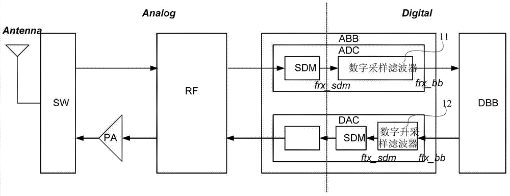
technical field [0001] The present invention relates to the technical field of wireless communication, and more specifically, relates to a digital filter and a configuration method thereof, electronic equipment and a wireless communication system. Background technique [0002] ABB (Analog Baseband, analog baseband) located between DBB (Digital Base band, digital baseband) and RF (Radio Frequency, radio frequency) in the current wireless terminal system supporting multi-mode communication. The more important function of the ABB is the conversion between analog and digital based on DAC (Digital Analog Converter, digital-to-analog converter) and ADC (Analog Digital Converter, analog-to-digital converter). [0003] Such as figure 1 Shown is the signal flow chart of the wireless terminal communication system, according to figure 1 The dotted line in the middle divides ABB into the analog signal processing part Analog (to the left of the dotted line) and the digital signal proce...

Claims


Application Information

Patent Timeline
IPC IPC(8): H03H17/02
Inventor 韦春妍刘永平邹定锴
Owner HUAWEI TECH CO LTD
Learn More