Check patentability & draft patents in minutes with Patsnap Eureka AI!

Method for Improving the Uniformity of Polysilicon Doping and Diffusion in SiGe Emitter

A technology of polysilicon and emitter, which is applied in the direction of electrical components, semiconductor/solid-state device manufacturing, circuits, etc., can solve the problems of uneven diffusion, unstable diffusion junction depth, etc., and achieve the effect of ensuring stability

Active Publication Date: 2016-04-13
SHANGHAI HUAHONG GRACE SEMICON MFG CORP
View PDF3 Cites 0 Cited by
  • Summary
  • Abstract
  • Description
  • Claims
  • Application Information

AI Technical Summary

Problems solved by technology

However, in order to ensure the uniform thickness of polysilicon in the furnace tube, different temperatures need to be set at different positions of the furnace tube, which leads to differences in the grain size of polysilicon at different positions in the furnace tube, resulting in subsequent polysilicon doping post-diffusion inhomogeneities, such as figure 1 As shown, the diffusion junction depth in the EB junction (emitter / base) is unstable, which eventually leads to problems with the stability of the emitter short-circuit current amplification factor β

Method used


Image

  • Method for Improving the Uniformity of Polysilicon Doping and Diffusion in SiGe Emitter
  • Method for Improving the Uniformity of Polysilicon Doping and Diffusion in SiGe Emitter
  • Method for Improving the Uniformity of Polysilicon Doping and Diffusion in SiGe Emitter

Examples


Embodiment Construction

[0010] In order to have a more specific understanding of the technical content, characteristics and effects of the present invention, now in conjunction with the illustrated embodiment, the details are as follows:

[0011] In this embodiment, the diffusion uniformity after polysilicon doping of the SiGe emitter is improved through the following process steps:

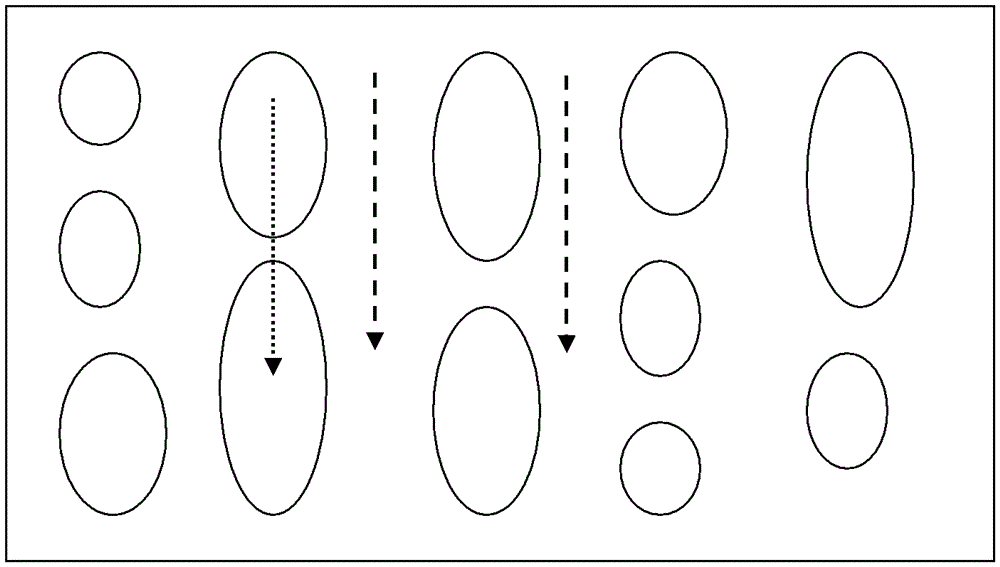
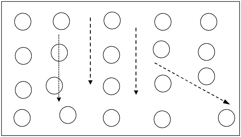
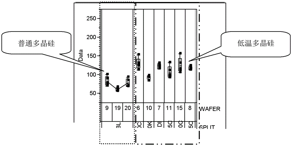
[0012] Firstly, when polysilicon is deposited by low-pressure chemical vapor deposition in the furnace tube, the average temperature of the furnace tube is set at a low temperature of 590-620° C., and the pressure is set at 300-800 mTorr. In the polysilicon film layer formed after such deposition, the grain size is small and uniform. After doping, the diffusion of impurities is mainly completed through the grain boundary, such as figure 2 As shown, since impurities diffuse less through the crystal grains, the diffusion speed of impurities in polysilicon is basically the same, so that a more stable EB junction depth and...


PUM


Abstract

The invention discloses a method for improving polycrystalline silicon doping diffusing uniformity of a germanium-silicon emitter. During low-pressure chemical gas phase polycrystalline silicon deposition, average furnace tube temperature is set at 590-620 DEG C. Polycrystalline silicon is deposited at low temperature, so that impurity diffusing uniformity after polycrystalline silicon doping of the germanium-silicon emitter is improved, and stability of short circuit current amplification factors of the germanium-silicon emitter is guaranteed.

Description

technical field [0001] The invention relates to the field of semiconductor integrated circuit manufacturing, in particular to a method for improving the uniformity of polysilicon doping and diffusion in a germanium-silicon emitter. Background technique [0002] The application of polysilicon doping process in semiconductors is very common. It can be said that almost all MOS devices have to have this part of the process. However, due to the large grain size in polysilicon, and the diffusion rate of doped impurities in the grains is very different from that in the grain boundary, the distribution of doped diffusion in polysilicon is very small. uneven. For ordinary MOS devices, due to the blocking of the gate oxide layer, after the subsequent annealing, the unevenness of this diffusion will not have a great impact on the characteristics of the device, but in the preparation process of special devices, the unevenness of this diffusion Inhomogeneity will obviously affect the s...

Claims


Application Information

Patent Timeline
Patent Type & Authority Patents(China)
IPC IPC(8): H01L21/223H01L21/20
Inventor 刘继全孙勤陈帆
Owner SHANGHAI HUAHONG GRACE SEMICON MFG CORP
Features
  • R&D
  • Intellectual Property
  • Life Sciences
  • Materials
  • Tech Scout
  • Unparalleled Data Quality
  • Higher Quality Content
  • 60% Fewer Hallucinations
Learn More