[0051] In order to make the objectives, technical solutions and advantages of the present invention clearer, the present invention will be described in detail below with reference to the accompanying drawings and specific embodiments.
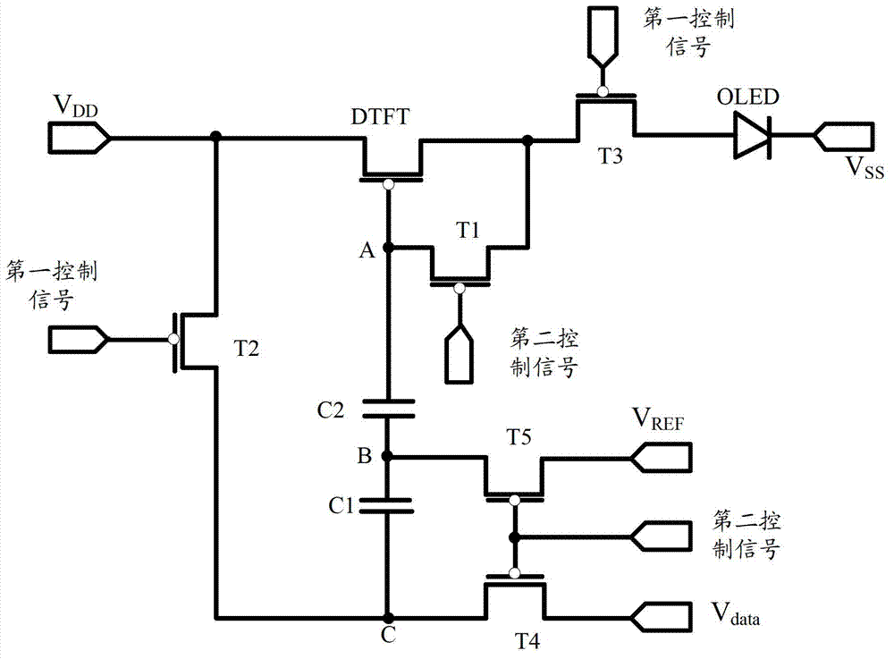
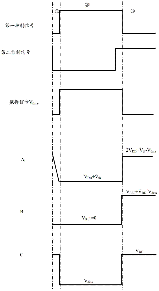
[0052] Such as Figure 7 As shown, the pixel circuit according to the specific embodiment of the present invention includes a first voltage signal terminal V DD And the second voltage signal terminal V SS A light-emitting device OLED and a driving transistor DTFT for driving the light-emitting device are connected in series, and the pixel circuit further includes a light-emitting control module and a compensation module, wherein:
[0053] The input end of the light emission control module is connected to a first control signal, and the output end is respectively connected to the source and drain of the driving transistor DTFT. The light emission control module is used to respond to the first control signal to control the The state of the driving transistor DTFT makes the light emitting device emit light or turn off;
[0054] The input terminal of the compensation module is connected with a second control signal, and the output terminal is respectively connected with the gate and source of the driving transistor DTFT and the light emission control module, and the compensation module is used to respond to the second control signal , Disconnecting or turning on the connection between the gate and the source of the driving transistor, so that the voltage at the gate of the driving transistor when the light emitting device OLED emits light compensates the threshold voltage of the driving transistor DTFT.
[0055] Wherein, the light emission control module specifically includes:
[0056] A second switching transistor, the gate of the second switching transistor is connected to the first control signal, and the source is connected to the drain of the driving transistor;
[0057] A third switch transistor, the gate of the third switch transistor is connected to the first control signal, and is used to disconnect or turn on the connection between the driving transistor and the light emitting device in response to the first control signal, The drain of the third switch transistor is connected to the source of the driving transistor, and the source of the third switch transistor is connected to the light emitting device;
[0058] The compensation module specifically includes:
[0059] A first capacitor and a second capacitor arranged in series between the drain of the second switching transistor and the gate of the driving transistor;
[0060] The first switching transistor is arranged between the gate and the source of the driving transistor, and the gate of the first switching transistor is connected to the second control signal, and is used for turning off in response to the second control signal. Or turn on the connection between the gate and the source of the driving transistor;
[0061] A fifth switch transistor, the gate of the fifth switch transistor is connected to the second control signal, the source of the fifth switch transistor is connected to a reference voltage, and the drain of the fifth switch transistor is connected to the first A common connection terminal between a capacitor and the second capacitor is connected;
[0062] The fourth switch transistor is arranged between the data signal terminal and the common connection terminal of the second switch transistor and the first capacitor, and the gate of the fourth switch transistor is connected to the second control signal, so The drain of the fourth switch transistor is connected to one end of the first capacitor, and the source of the fourth switch transistor is connected to a data signal.
[0063] According to a pixel circuit according to a specific embodiment of the present invention, a second switching transistor, a first capacitor, and a second capacitor are sequentially arranged in series between the first voltage signal terminal and the gate of the driving transistor, and the The gate of the second switching transistor is connected to the first control signal, and is used to disconnect or turn on the connection between the gate and the drain of the driving transistor in response to the first control signal;
[0064] Through a third switching transistor provided between the second voltage signal terminal and the source of the driving transistor, the gate of the third switching transistor is connected to the first control signal for responding to the first control signal. A control signal to disconnect or turn on the connection between the driving transistor and the light emitting device;
[0065] Through the first switching transistor provided between the gate and the source of the driving transistor, the gate of the first switching transistor is connected to a second control signal for turning off or Turn on the connection between the gate and the source of the driving transistor.
[0066] The pixel circuit controls the input of the first control signal and the second control signal, so that the driving transistor used to drive the light-emitting device to emit light has different states at different stages, so that the threshold voltage of the driving transistor V th It can be reflected by the voltage at point A at the gate of the driving transistor. When the light-emitting device emits light, the second capacitor C2 is used to compensate the threshold voltage V of the driving transistor. th , So as to ensure the uniformity of the luminous brightness of the light-emitting device.
[0067] Preferably, the third reference voltage is connected to ground.
[0068] In addition, the light emitting device is connected in series between the second voltage signal terminal and the third switch transistor.
[0069] The specific structure of the pixel circuit of the present invention will be described in detail below.
[0070] Such as figure 2 Shown is a schematic structural diagram of the pixel circuit of the present invention. Refer to figure 2 As shown, the pixel circuit structure of this embodiment contains 6 TFTs (Thin Film Transistor, thin film field effect transistors) and 2 capacitors C. Among them, the 6 TFTs are all P-channel transistors, and T1 to T5 are switching transistors. DTFT is a driving transistor. In the following description, for T1 to T5 and the driving transistor, the source and drain are defined by the flow direction of the reference current, the inflow of current is used as the drain, and the outflow is used as the source. In addition, this embodiment uses two control signals, one data signal V data , Three voltage signals V DD , V SS , V REF.
[0071] Such as figure 2 As shown, at the first voltage signal terminal V DD And the second voltage signal terminal V SS The light-emitting device OLED and the driving transistor DTFT for driving the light-emitting device OLED are connected in series, and T2, C1, and C2 are connected in series between the first voltage signal terminal and the gate of the DTFT, and the gate and source of the DTFT are connected in series. T1 is connected in series between the sources of OLED and DTFT, and the data signal V is connected between the common connection terminal of T2 and C1. data T4 is connected in series between C1 and C2 and the reference voltage V REF T5 is connected in series. Among them, the gates of T2 and T3 are respectively used to receive the first control signal, and in response to the first control signal, turn off or on; the gates of T1, T4, and T5 are respectively used to receive the second control signal and respond to the first control signal. The second control signal is disconnected or turned on. In the specific embodiment of the present invention, the gates of T4 and T5 are connected and simultaneously connected to the second control signal.
[0072] Combine below image 3 The timing diagram shown, right figure 2 The working flow of the pixel circuit structure shown is introduced in detail:
[0073] 1) The first stage shown in the timing diagram is the pixel reset stage: the first control signal is low, the second control signal is low, and the data signal V data It is low level. Refer to Figure 4 Show the equivalent circuit of the first stage at this time, at this time T1 to T5 are all on. At this time, because T1 is turned on, DTFT is in a diode link state. At this time, the drain voltage of DTFT is V DD +V th. At the end of stage ①, the potential of point A reaches V DD +V th , The potential of point B is V REF , The potential of point C is V DD. In the specific embodiment of the present invention, the third voltage signal terminal V REF Ground connection, so V REF Is zero.
[0074] 2) The second stage shown in the timing diagram is the data writing stage: at this time, the first control signal is at a high power level, the second control signal is at a low level, and the data signal V data It is high level. Refer to Figure 5 The equivalent circuit of stage ② is shown. At this time, T1, T4 and T5 are turned on, and T2, T3 are turned off. Since T1 connected in series between the gate and source of the DTFT is turned on, the DTFT continues to maintain the diode connection state, and the potential at point A remains unchanged; because T5 is turned on, the potential at the common connection terminal B of C1 and C2 V REF Is zero; because T2 is off and T4 is on, the potential at the common connection terminal C of T2 and C1 is V data , C1 and C2 are both in the charging state.
[0075] 3) The third stage shown in the timing diagram is the light-emitting stage: at this time, the first control signal is at low level, the second control signal is at high level, and the data signal V data It is low level. Refer to Image 6 As shown in the equivalent circuit diagram of stage ③, T1, T4, and T5 are disconnected, and T2 and T3 are turned on. Since T2 is turned on, the potential at the common connection terminal C of T2 and C1 becomes V DD , Because T5 is disconnected, C1 and C2 share the same electrode, and the potential at point B increases to V REF +V DD -V data , At the same time the potential of point A is increased to 2V DD +V th -V data. At this time, for DTFT, the voltage difference between the gate and the source V gs =V DD +V th -V data , DTFT is in saturation at this time, charging the light-emitting device OLED, and the output current is:
[0076] I = 1 2 β ( V gs - V th ) 2 = 1 2 β ( VDD + V th - DATA - V th ) 2 = 1 2 β ( VDD - DATA ) 2
[0077] Therefore, at this time, the current on the light-emitting device OLED and the threshold voltage V of the DTFT th Regardless, the driving current of the OLED can be kept stable, thereby improving the uniformity of the panel brightness.
[0078] In the pixel circuit described in the specific embodiment of the present invention, the V of the DTFT is th The information feedback is the potential of point A at the gate of the DTFT, and the C2 storage method is used to compensate the V of the DTFT th The difference makes the drive current I and V of the drive tube th Regardless, the stability of the drive current is achieved, and the uniformity of the panel brightness is improved.
[0079] Another aspect of the present invention also provides a method for driving the above-mentioned pixel circuit, the method including:
[0080] In the first stage, the first control signal and the second control signal are applied, the light emission control module responds to the first control signal, and the compensation module responds to the second control signal to enable the drive transistor The gate is connected to the drain;
[0081] In the second stage, the first control signal and the second control signal are applied, the light emission control module responds to the first control signal, and the compensation module responds to the second control signal to enable the drive transistor Keep the gate and drain connected;
[0082] In the third stage, the first control signal and the second control signal are applied, the light emission control module responds to the first control signal, and the compensation module responds to the second control signal to enable the drive transistor When saturated, the light emitting device emits light.
[0083] The light emission control module specifically includes:
[0084] A second switching transistor, the gate of the second switching transistor is connected to the first control signal, and the source is connected to the drain of the driving transistor;
[0085] A third switch transistor, the gate of the third switch transistor is connected to the first control signal, and is used to disconnect or turn on the connection between the driving transistor and the light emitting device in response to the first control signal, The drain of the third switch transistor is connected to the source of the driving transistor, and the source of the third switch transistor is connected to the light emitting device;
[0086] The compensation module specifically includes:
[0087] A first capacitor and a second capacitor arranged in series between the drain of the second switching transistor and the gate of the driving transistor;
[0088] The first switching transistor is arranged between the gate and the source of the driving transistor, and the gate of the first switching transistor is connected to the second control signal, and is used for turning off in response to the second control signal. Or turn on the connection between the gate and the source of the driving transistor;
[0089] A fifth switch transistor, the gate of the fifth switch transistor is connected to the second control signal, the source of the fifth switch transistor is connected to a reference voltage, and the drain of the fifth switch transistor is connected to the first A common connection terminal between a capacitor and the second capacitor is connected;
[0090] The fourth switch transistor is arranged between the data signal terminal and the common connection terminal of the second switch transistor and the first capacitor, and the gate of the fourth switch transistor is connected to the second control signal, so The drain of the fourth switch transistor is connected to one end of the first capacitor, and the source of the fourth switch transistor is connected to a data signal;
[0091] Wherein, in the first stage, the first switch transistor, the second switch transistor, the third switch transistor, the fourth switch transistor, and the fifth switch transistor are all turned on;
[0092] In the second stage, the first switching transistor, the fourth switching transistor, and the fifth switching transistor are turned on, and the second switching transistor and the third switching transistor are turned off;
[0093] In the third stage, the first switch transistor, the fourth switch transistor, and the fifth switch transistor are turned off, and the second switch transistor and the third switch transistor are turned on.
[0094] Preferably, in the first stage, the first control signal and the second control signal output a low level, and the data signal outputs a low level; in the second stage, the first control signal The signal outputs a high level, the second control signal outputs a low level, and the data signal outputs a high level; in the third stage, the first control signal outputs a low level, and the second control signal A high level is output, and the data signal is a low level.
[0095] In the method, the driving transistor used to drive the light-emitting device to emit light has different states at different stages by controlling the input first control signal and the second control signal, so that the threshold voltage V of the driving transistor is th It can be reflected by the voltage at point A at the gate of the driving transistor. When the light-emitting device emits light, the second capacitor C2 is used to compensate the threshold voltage V of the driving transistor. th , So as to ensure the uniformity of the luminous brightness of the light-emitting device.
[0096] The above are only the preferred embodiments of the present invention. It should be pointed out that for those of ordinary skill in the art, without departing from the principle of the present invention, several improvements and modifications can be made, and these improvements and modifications are also It should be regarded as the protection scope of the present invention.