Flip-chip welding spot defect detection method through temperature observation and measurement

A flip-chip and flip-chip welding technology, which is applied in the field of detection of chip solder joint defects, can solve the problems that the detection technology cannot meet the actual needs of production, and achieve the effects of a wide range of applicable processes, intuitive and simple discrimination, and a high defect recognition rate

Inactive Publication Date: 2013-07-10
HARBIN INST OF TECH
View PDF3 Cites 11 Cited by
  • Summary
  • Abstract
  • Description
  • Claims
  • Application Information

AI Technical Summary

Problems solved by technology

[0009] Aiming at the defect that the existing detection technology cannot meet the actual demand of production, the present invention provides a reliable detection method for visual temperature measurement of solder joint defects of flip-chip

Method used


Image

  • Flip-chip welding spot defect detection method through temperature observation and measurement
  • Flip-chip welding spot defect detection method through temperature observation and measurement
  • Flip-chip welding spot defect detection method through temperature observation and measurement

Examples


Embodiment Construction

[0025] The technical solution of the present invention will be further described below in conjunction with the accompanying drawings, but it is not limited to this. Any modification or equivalent replacement of the technical solution of the present invention without departing from the spirit and scope of the technical solution of the present invention should be covered by the technical solution of the present invention. in the scope of protection.

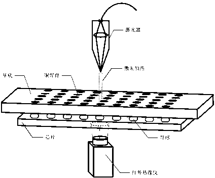
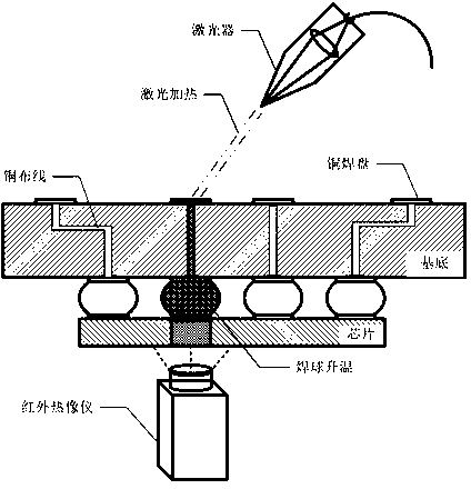
[0026] Such as figure 1 As shown, a thermal imager is set on the chip side of the flip chip, the infrared laser is placed on the substrate side, and the diameter of the laser beam is slightly smaller than that of the pad. Aim the infrared laser beam at the pad to be tested on the flip chip substrate, adjust the power and pulse width parameters, and apply thermal excitation to it, that is, input a fixed amount of heat to the pad, during which the temperature of the pad rises rapidly The thermal imager detects the temperature rise ...


PUM


Abstract

The invention provides a flip-chip welding spot defect detection method through temperature observation and measurement, and relates to a flip-chip welding spot defect detection method. The method includes the steps of: arranging a thermal imaging system at one side of a flip chip, arranging an infrared laser at one side of a substrate, aligning an infrared laser beam to a to-be-detected welding disc of the substrate of the flip chip, adjusting power and pulse width parameters and performing thermal excitation on the power and pulse width, wherein the thermal imaging system detects the temperature rising process of a chip ball-welding zone connected with the welding disc in real time, observes and shoots a thermal image of a highest temperature rising point, and judges a flip-chip welding spot defect according to the temperature rising curve or the thermal image. The flip-chip welding spot defect detection method for empty welding adopts point-by-point detection and has the characteristics of no damage, high defect recognition rate and simplicity and intuition in judgment; and besides, the method has a wide application range, can be suitable for the detect detection in chip side ball placement and the detect detection in substrate side ball placement during three-dimensional assembly.

Description

technical field [0001] The invention relates to a detection method for chip solder joint defects, in particular to a detection method for flip-chip solder joint defects. Background technique [0002] With the development of electronic packaging technology in the direction of high density, high performance and miniaturization, BGA (Ball Grid Array) packaging has become the mainstream of contemporary electronic packaging. Ceramic ball grid array CBGA (CeramicBall Grid Array), as a packaging form of BGA, is widely used in military, aviation and aerospace electronic equipment manufacturing fields due to its high I / O density, high reliability and good electrical and thermal performance . CCGA (Ceramic Column Grid Array) is an improvement based on CBGA. It replaces the ball array with a column array, which relieves the shear stress between the ceramic substrate and the PCB caused by thermal mismatch, and improves thermal cycle reliability. [0003] The miniaturization of microel...

Claims


Application Information

Patent Timeline
Patent Type & Authority Applications(China)
IPC IPC(8): H01L21/66
Inventor 田艳红孔令超王春青刘威刘宝磊
Owner HARBIN INST OF TECH
Why Eureka
Try Eureka