Thin film transistor array substrate and manufacturing method thereof

A technology for thin film transistors and array substrates, applied in the field of thin film transistor array substrates and their manufacturing, can solve the problems of complex structure, reducing pixel aperture ratio, limiting the arrangement and area of ​​pixel electrodes 21, etc. rate, and the effect of improving product performance

Active Publication Date: 2013-07-10
EVERDISPLAY OPTRONICS (SHANGHAI) CO LTD
View PDF2 Cites 24 Cited by
  • Summary
  • Abstract
  • Description
  • Claims
  • Application Information

AI Technical Summary

Problems solved by technology

[0006] In the above-mentioned traditional thin film transistor array, the initialization power line 14 and the pixel electrode 21 are the same layer of metal, and the pattern is formed by the same photolithography process. The arrangement and area of ​​the pixel electrodes 21 on the array substrate are reduced, that is, the aperture ratio of the pixels is reduced; moreover, the vapor deposition of red, green and blue materials in the direction perpendicular to the initialization power line 14 is also limited, and the product The luminous brightness cannot be maximized; at the same time, the structure of the contact hole 20 in the pixel is complicated, and three photolithography processes are required to realize the electrical connection. Because the size of the hole in the pixel is small, it is easy to have poor contact between the pixel electrode 27 and the semiconductor. Problems that affect product yield

Method used


Image

  • Thin film transistor array substrate and manufacturing method thereof
  • Thin film transistor array substrate and manufacturing method thereof
  • Thin film transistor array substrate and manufacturing method thereof

Examples


Embodiment Construction

[0067] Specific embodiments of the present invention will be described in detail below. It should be noted that the embodiments described here are for illustration only, and are not intended to limit the present invention.

[0068] Thin Film Transistor Array Substrate

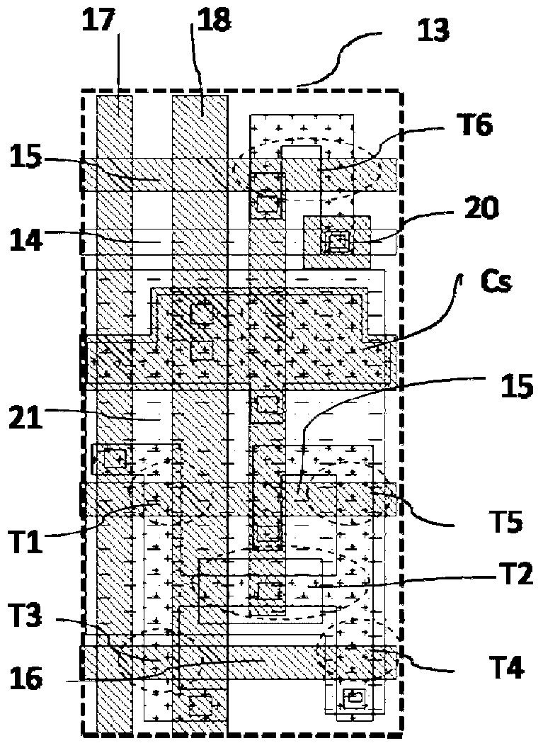
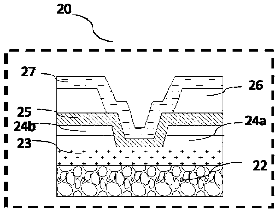
[0069] Such as Figure 4 As shown, the TFT array substrate for driving organic light emitting diodes of the present invention includes a substrate 22, an insulating layer formed on the substrate 22, a power line 18, a data line 17 and an initialization power line 14 formed on the insulating layer, The planarization layer 26 covering the power supply line 18 , the data line 17 and the initialization power supply line 14 , and the pixel electrodes formed on the planarization layer 26 .

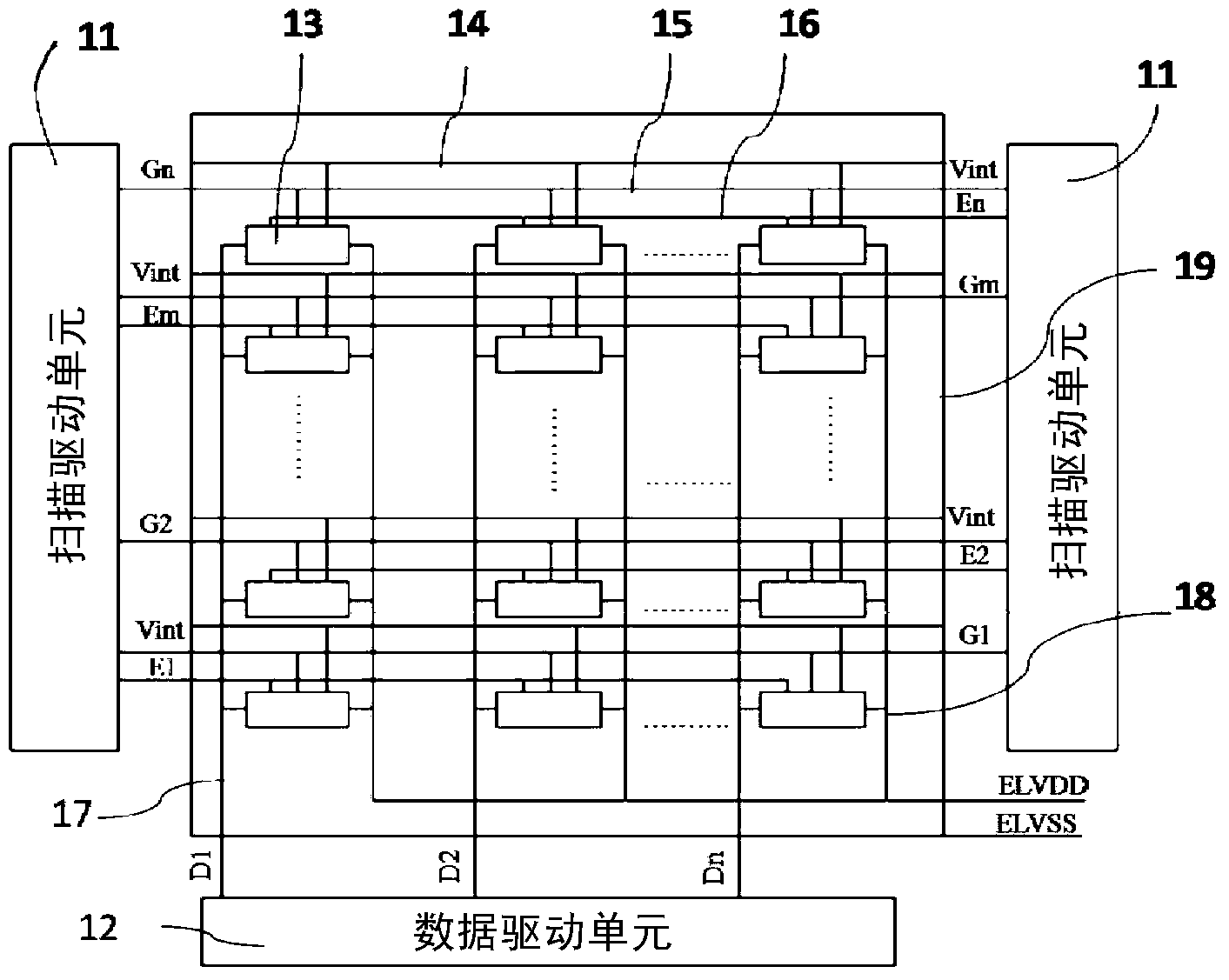
[0070] Further, the TFT array substrate of the present invention further includes a scanning line driving unit 11 , a data line driving unit 12 and a plurality of pixels 13 .

[0071] The scanning line driving unit 11 includes...


PUM


Abstract

The invention provides a thin film transistor array substrate and a manufacturing method thereof. The thin film transistor array substrate comprises a substrate, an insulating layer, a power line, a data line, an initialized power line, a planarization layer and a pixel electrode, wherein the insulating layer is formed on the substrate; the power line, the data line and the initialized power line are all formed on the insulating layer; the planarization layer is covered on the power line, the data line and the initialized power line; and the pixel electrode is formed on the planarization layer. According to the invention, the initialized power line and the data line are on the same metal layer, while the initialized power line is not on the layer on which the pixel electrode is located, so that the initialized power line does not occupy the lining space of the pixel electrode, the pixel area can be maximized, thus the pixel aperture opening ratio can be improved greatly, the effective light-emitting area can be improved and the product performance can be improved.

Description

technical field [0001] The invention relates to a thin film transistor array substrate and a manufacturing method thereof. Background technique [0002] Organic light-emitting diode (OLED) display technology is different from the traditional LCD display method. It has the characteristics of self-illumination. It can be made lighter and thinner, with a wider viewing angle and more vivid colors. It has the incomparable advantages of LCD. In recent years OLED applications are becoming more and more widespread. [0003] Such as figure 1 As shown, the existing TFT array substrate for driving organic light emitting diodes includes a scan driving unit 11 , a data line driving unit 12 and a plurality of pixels 13 . Each pixel unit 13 corresponds to an initialization power line 14 . The initialization power line 14 is arranged in parallel with the scanning line 15 and the light emission control line 16 (E1˜En). The initialization power line 14 is vertically arranged with the data...

Claims


Application Information

Patent Timeline
Patent Type & Authority Applications(China)
IPC IPC(8): H01L27/12H01L21/77H01L27/32
Inventor 汪梅林秦永亮
Owner EVERDISPLAY OPTRONICS (SHANGHAI) CO LTD
Why Eureka
Try Eureka