Array substrate, manufacture method of array substrate and display device

A technology for array substrates and substrates, which is used in semiconductor/solid-state device manufacturing, electrical components, and electrical solid-state devices, etc., and can solve the problems of high production cost and low yield rate.

Active Publication Date: 2013-07-17
BOE TECH GRP CO LTD +1
View PDF6 Cites 49 Cited by
  • Summary
  • Abstract
  • Description
  • Claims
  • Application Information

AI Technical Summary

Problems solved by technology

[0005] However, since the number of patterning processes directly affects the production cost and the yield rate, the more the patterning process, the longer the production cycle, the higher the production cost, and the lower the yield rate

Method used


Image

  • Array substrate, manufacture method of array substrate and display device
  • Array substrate, manufacture method of array substrate and display device
  • Array substrate, manufacture method of array substrate and display device

Examples


Embodiment 1

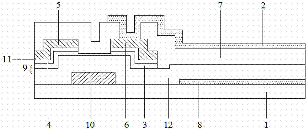
[0102] An embodiment of the present invention provides an array substrate. As shown in FIGS. , the source electrode 151, the drain electrode 152 and the insulating protection layer 16, the pixel electrode 111 and the common electrode 171 are also arranged on the substrate 10, and the first lead hole 20 connecting the pixel electrode 111 and the drain electrode 152 and connecting the common electrode 171 and the common The second lead hole 21 of the electrode line 122, wherein, the pixel electrode 111 is arranged on the substrate 10, the grid 121 is directly arranged on the transparent conductive layer arranged on the same layer as the pixel electrode 111; the pixel electrode 111 is arranged through the first lead hole The first metal connection layer 123 in 20 is connected to the drain electrode 152 , and the first metal connection layer 123 and the gate 121 are arranged on the same layer.

[0103] Preferably, the common electrode line 122 and the gate electrode 121 in this em...

Embodiment 2

[0124] An embodiment of the present invention also provides a display device, which includes any one of the array substrates described in Embodiment 1. The display device may be any product or component with a display function such as a liquid crystal panel, an electronic paper, an OLED panel, a mobile phone, a tablet computer, a television, a monitor, a notebook computer, a digital photo frame, a navigator, and the like.

[0125] In the display device provided by the embodiments of the present invention, the number of patterning processes used in the preparation process of the array substrate used is reduced, thereby effectively reducing the manufacturing cost and improving the yield rate.

Embodiment 3

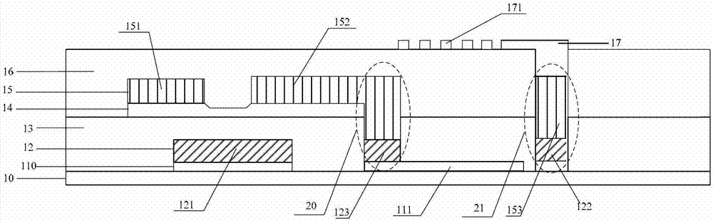
[0127] The embodiment of the present invention also provides a method for manufacturing an array substrate, such as Figure 6 shown, including:

[0128] 101. Form a pixel electrode, a gate, a first metal connection layer, a common electrode line, a gate insulating layer, an active layer, a first lead hole 20 and a second lead hole 21 through the first patterning process;

[0129] As shown in Fig. 7(a) and (b), a transparent conductive film and a gate metal film are deposited on the substrate 10, and then a multi-level masking process is performed for sub-regional exposure and sub-regional etching to form the pixel electrode layer 11. Pattern (comprising pixel electrode 111) and the pattern of gate metal layer 12, the pattern of gate metal layer 12 comprises gate 121, gate line, the first metal connection layer 123 that is positioned at the first lead hole 20, and common electrode line 122 , the common electrode line partially extends to a position corresponding to the second ...


PUM


Abstract

The invention discloses an array substrate, a manufacture method of the array substrate and a display device and relates to the display field. The using times of a picture composition process in the array substrate manufacture process can be decreased, accordingly the manufacture cost if effectively reduced, and the yield is improved. The array substrate comprises a substrate body, a grid electrode, a grid insulating layer, an active layer, a source electrode, a drain electrode and an insulation protecting layer, wherein the grid electrode, the grid insulating layer, the active layer, the source electrode, the drain electrode and the insulation protecting layer are sequentially arranged on the substrate body. A pixel electrode, a public electrode, a first lead wire hole connected with the pixel electrode and the drain electrode and a second lead wire hole connected with the public electrode and a public electrode wire are further arranged on the substrate body, the pixel electrode is arranged on the substrate body, and the grid electrode is directly arranged on a transparent conducting layer which is arranged on the same layer together with the pixel electrode. The pixel electrode is connected with the drain electrode through a first metal connecting layer arranged in the first lead wire hole, and the first metal connecting layer and the grid electrode are arranged on the same layer.

Description

technical field [0001] The present invention relates to the display field, in particular to an array substrate, a manufacturing method thereof, and a display device. Background technique [0002] Advanced-Super Dimensional Switching (abbreviation: ADS) forms a multi-dimensional electric field through the parallel electric field generated by the edge of the pixel electrode or the common electrode in the same plane and the vertical electric field generated between the pixel electrode and the common electrode, so that the liquid crystal cell All alignment liquid crystal molecules between the inner pixel electrodes or the common electrodes, and directly above the pixel electrodes or the common electrodes can produce rotation conversion, thereby improving the working efficiency of the plane alignment liquid crystal and increasing the light transmission efficiency. Advanced ultra-dimensional field switching technology can improve the picture quality of TFT-LCD, and has the advanta...

Claims


Application Information

Patent Timeline
Patent Type & Authority Applications(China)
IPC IPC(8): H01L27/02H01L21/77
CPCH01L21/77H01L29/02H01L27/124H01L27/1262H01L27/1288
Inventor 吴松包杰琼
Owner BOE TECH GRP CO LTD
Why Eureka
Try Eureka