Printing antenna
A technology for printing antennas and antenna patterns, which is applied in the field of wireless communication, can solve the problems of large equipment investment, large capital occupation, and increased production difficulty, and achieve the effects of reducing additional investment, utilizing the printing area, and eliminating chemical plating and plating pollution
- Summary
- Abstract
- Description
- Claims
- Application Information
AI Technical Summary
Problems solved by technology
Method used
Image

Examples
Embodiment 1
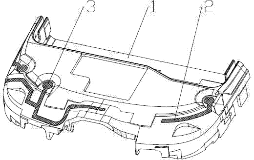
[0023] The upper and lower surfaces of the plastic housing in this embodiment are respectively distributed with antenna patterns 2 formed by printing conductive ink; the plastic housing is provided with a through hole 4 that runs through the upper and lower surfaces, and the printed on The antenna patterns on the upper and lower surfaces extend into the through hole and are connected to form a continuous conductive path.
[0024] The antenna pattern is printed and distributed on the plane or three-dimensional curved surface of the upper and lower surfaces of the plastic shell.
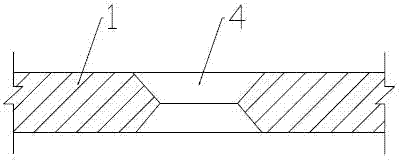
[0025] In this embodiment, as attached figure 2 As shown, the through hole is a tapered hole, and the ratio of the radius to the depth of the tapered hole is at least 2:1. Preferably, the maximum diameter-to-depth ratio of the tapered hole is (2-10): 1; the antenna pattern printed on the upper and lower surfaces of the plastic casing extends to the inner wall of the through hole and is connected to f...
Embodiment 2
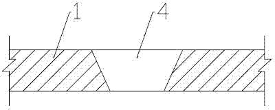
[0033] The difference between the present embodiment and the first embodiment is that the openings on both sides of the through hole 4 are tapered, that is, they are bell-mouthed, and the ratio of the radius to the depth is at least 2:1. Preferably, the maximum diameter-to-depth ratio of the through hole is (2-10): 1; the antenna pattern printed on the upper and lower surfaces of the plastic housing extends to the inner wall of the through hole and is connected to form a continuous conductive line. path. . as attached image 3 As shown, the maximum diameter-to-depth ratio of the through hole is 2:1, and the slope ratio of the bell mouth on both sides is 1:0.3; the tapered hole design of the through hole is also to facilitate the printing of conductive lines, and at the same time, the through hole It can be used as a conduction path for other circuits between the two sides of the plastic casing of the electronic device.
Embodiment 3
[0035] The difference between this embodiment and Embodiment 1 is that: Figure 4 As shown, a copper post 3 is embedded in the plastic case, and one end surface of the copper post is flush with the upper or lower surface of the plastic case; the antenna pattern printed on the upper or lower surface of the plastic case extends to the copper post. The end face of the post and the copper post jointly form a conductive path.
[0036] In an application of this embodiment, the antenna patterns printed on the upper and lower surfaces extend to the end faces of the copper pillars to form a conductive path together with the copper pillars, and the antenna patterns on the upper and lower surfaces are connected through the copper pillars.
[0037]In another application of this embodiment, the antenna pattern printed on the upper or lower surface of the plastic casing on the plane or the three-dimensional curved surface extends to the end face of the copper column and is connected to form...
PUM
 Abstract
Description
Claims
Application Information
 - R&D
- Intellectual Property
- Life Sciences
- Materials
- Tech Scout
- Unparalleled Data Quality
- Higher Quality Content
- 60% Fewer Hallucinations
Browse by: Latest US Patents, China's latest patents, Technical Efficacy Thesaurus, Application Domain, Technology Topic, Popular Technical Reports.
© 2025 PatSnap. All rights reserved.Legal|Privacy policy|Modern Slavery Act Transparency Statement|Sitemap|About US| Contact US: help@patsnap.com