Method for preparing compound electrode

A technology of composite electrodes and printed electrodes, which is applied in the direction of chemical instruments and methods, circuits, electrical components, etc., can solve problems such as cost control, achieve the effects of reducing usage, easy understanding, and widening the range of choices

Inactive Publication Date: 2011-01-19
SUZHOU INST OF NANO TECH & NANO BIONICS CHINESE ACEDEMY OF SCI
View PDF8 Cites 37 Cited by
  • Summary
  • Abstract
  • Description
  • Claims
  • Application Information

AI Technical Summary

Problems solved by technology

[0003] However, in actual production, a problem worthy of attention is cost control

Method used


Image

  • Method for preparing compound electrode
  • Method for preparing compound electrode
  • Method for preparing compound electrode

Examples


Embodiment 1

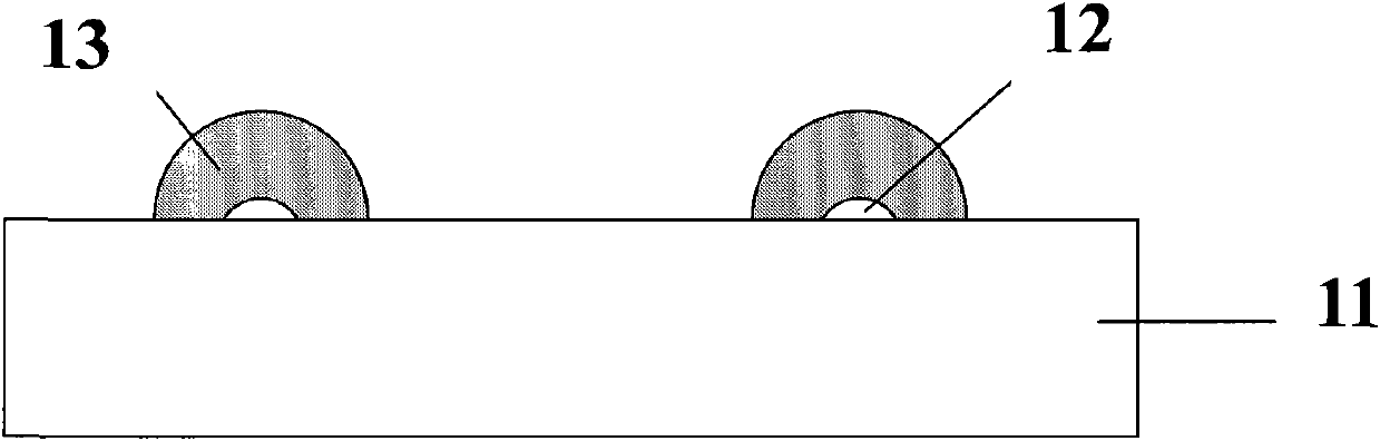
[0022] The front electrode of the solar cell generally uses a printed silver electrode with a mesh structure, which requires thin lines and good conductivity. In view of the fact that the conductivity of electroplated copper is much higher than that of printed silver electrodes and the cost is low, silver-copper composite electrodes can be used to balance the requirements of work function, conductivity and cost.

[0023] The sectional schematic diagram of silver-copper composite electrode in the present embodiment is as follows figure 1 shown. Crystalline silicon wafers are first cleaned, textured, phosphorous diffused, and silicon nitride film deposited by PECVD in accordance with solar cell manufacturing process standards. Print the special silver paste for solar cells on the silicon nitride film of the obtained silicon wafer 11 by air jet printing method to form a mesh silver electrode 12 with a width of about 10 microns and a thinner (thickness is about 1 micron), and the...

Embodiment 2

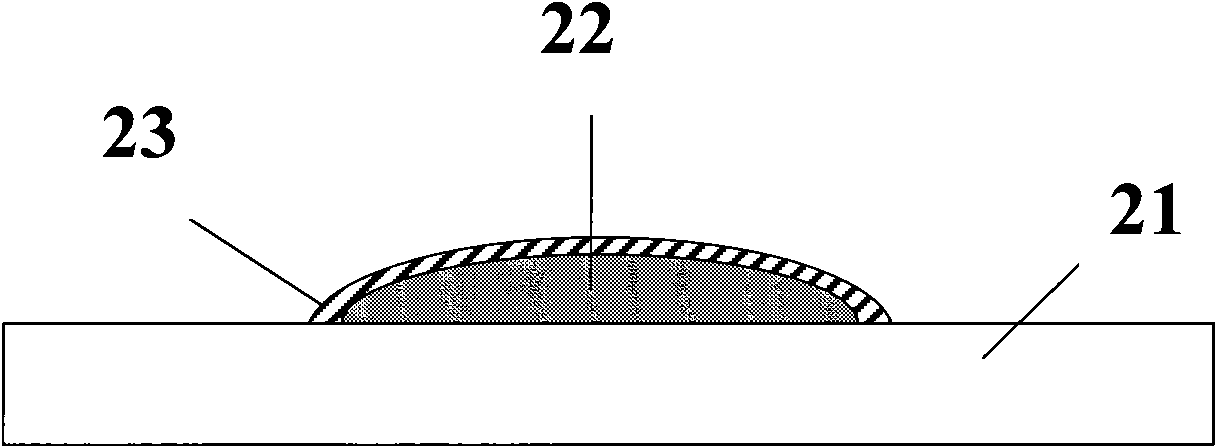
[0027] Considering factors such as work function and oxidation stability, current organic field-effect transistors on flexible substrates generally use gold as the gate electrode, so a large amount of expensive high-purity gold will be consumed in the preparation of large-area transistor arrays. At the same time, it is necessary to ensure a vacuum atmosphere to obtain the transistor gate electrode by the vacuum deposition method, which is costly and time-consuming. Even if the printing method is adopted, the price of gold paste or gold ink also determines that the preparation of such a gold electrode by the printing method is also expensive and has poor conductivity. The use of aluminum-gold electrodes as the gate electrodes of the field effect transistors on the flexible substrate can reduce the cost while taking into account the performance of the electrodes.

[0028] In this embodiment, the schematic cross-sectional view of the aluminum-gold composite electrode as the gate ...

Embodiment 3

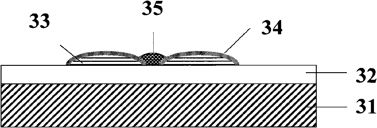
[0032] As described in Example 2, if the composite electrode used as the gate electrode of the organic field effect transistor is required to have a thickness less than 2 microns, a printed silver electrode can be used as the bottom layer of the composite electrode.

[0033] A 30 picoliter nozzle was selected to inkjet print 50% solid content silver ink with a thickness of 2 microns at a pitch of 25 microns on a cleaned and surface-treated flexible substrate, and the temperature of the workbench was set at 60 degrees Celsius. The printed sample is dried and sintered at 150 degrees Celsius to form a silver grid electrode with a thickness of less than 1 micron. Then immerse the flexible substrate that has been activated on the gate electrode into a plating tank filled with gold plating solution for chemical gold plating, strictly control the speed and progress of the reaction, and take it out when the thickness of the gold plating layer is 0.1 to 0.15 microns. The precautions of...


PUM

PropertyMeasurementUnit
thicknessaaaaaaaaaa
widthaaaaaaaaaa

Abstract

The invention relates to a method for preparing a compound electrode, which aims to widen the selection range of electrode materials and simplify a production process so as to obtain the electrode with the best cost performance and reduce the using amount of noble metal. The method comprises the following steps of: selecting a semiconductor or insulated material as a substrate of the compound electrode; obtaining a printing electrode layer on the first layer of the bottom part of the compound electrode on the substrate by a printing process, and solidifying the printing electrode layer; and finally, obtaining electrode parts on the second layer or above the second layer of the compound electrode on the printing electrode layer by a plating process, wherein the plating process comprises electronic plating and chemical plating. The compound electrode prepared by the method is made of two or more layers of different conducting materials, and the preparation method combines the advantages of preparing electrodes by an electronic plating method and a printing method and can be widely applied to the field of printing electronics.

Description

technical field [0001] The invention relates to a method for preparing a metal electrode, in particular to a method for preparing an electrode on a semiconductor or insulating material, wherein the electrode is a composite structure of two or more layers of different materials, in order to take into account cost, conductivity and work function matching aspect requirements. Background technique [0002] In the past few decades, reducing costs and improving cost performance has always been the driving force for the continuous development and growth of the electronics industry. Compared with the traditional processing technology, the printing method has the advantages of saving raw materials, simple process, less environmental pollution, etc., and it is easy to realize large-area devices, which is more conducive to meeting the requirements of the electronics industry to reduce costs and expand the market. However, even with the world's top nano-conductive silver ink, the condu...

Claims


Application Information

Patent Timeline
Patent Type & Authority Applications(China)
IPC IPC(8): H01L31/18B32B15/01H01L51/56
CPCY02P70/50
Inventor 林剑崔铮
Owner SUZHOU INST OF NANO TECH & NANO BIONICS CHINESE ACEDEMY OF SCI
Why Eureka
Try Eureka