
Design method of clock tree structure based on soc chip

A design method and tree structure technology, applied in the direction of generating/distributing signals, etc., can solve the problems of consuming circuit routing resources, etc., and achieve the effects of saving clock circuit resources, reducing area loss, and increasing the operating frequency

Active Publication Date: 2016-06-01
FUZHOU ROCKCHIP SEMICON
View PDF2 Cites 0 Cited by
  • Summary
  • Abstract
  • Description
  • Claims
  • Application Information

AI Technical Summary

Problems solved by technology

[0005] The disadvantage of the above-mentioned prior art is that: the common clock part of the synchronous clock is very short, most of the synchronous clocks are routed separately, and all clocks are routed separately, which consumes circuit routing resources

Method used


Image

  • Design method of clock tree structure based on soc chip
  • Design method of clock tree structure based on soc chip
  • Design method of clock tree structure based on soc chip

Examples


Embodiment Construction

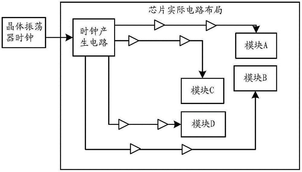
[0024] by image 3 and Figure 4 In contrast, the triangle in the figure is a buffer in the clock circuit, which is used to enhance the clock driving capability and control the clock delay, and the figure mainly indicates the delay length of the clock.

[0025] Module A and Module B use synchronous clocks. Assuming that the chip requires a performance of 500MHz, and each clock needs 2ns, if the source clock reaches the clock of module A and the clock of module B is exactly the same without any phase deviation, then each module has a margin of 2ns for functional timing. However, in the actual circuit, the two clocks need to be routed separately. Due to the reasons described above, the clock that finally reaches module A and the clock of module B cannot be completely consistent. When designing the module circuit, the clock routing difference needs to be deducted. For example, the module In the worst case, the clock of A and the clock of module B will differ by 0.5ns, so only a...


PUM


Abstract

The invention relates to a method for designing an SOC (System on Chip)-based clock tree structure. The method comprises the following steps of: finding common circuit portions on a synchronous clock path, and extracting the common portions, so that the common portions serve as a first-grade clock generation circuit; putting all branch clock generation circuits, except for the first-grade clock generation circuit, in a second-grade clock generation circuit; if common portions of common circuits of subsequent branch circuits exist in the second-grade clock generation circuit, reserving the common portions of the common circuits of the subsequent branch circuits, and putting all branch clock generation circuits, except for the first-grade clock generation circuit and the second-grade clock generation circuit, in a third-grade clock generation circuit; and continuously carrying out recursive grading in such a manner until common portions of the branch circuits do not exist any more. According to the method, a common clock portion of synchronous clocks is maximized, so that the clock tree structure is more optimized, the quality of clocks is improved, the eventual workable frequency increase of a chip is benefited, and the circuit resources of the clocks are saved.

Description

【Technical field】 [0001] The invention relates to a design method of clock tree structure based on SOC chip. 【Background technique】 [0002] A clock tree is a network structure built in balance by many buffer cells in a digital chip. It has a source point, usually a clock input port (clock input port), or a cell output pin (cell output pin) inside the design. Then it is built by level-by-level buffer units. The specific number of levels depends on your settings and the units used. The purpose is to make the clock skew of the terminal used (clockskew, generally the most concerned), insert delay When (insertiondelay) and transition (transition) to meet the design requirements. [0003] For a large digital chip, the frequency at which the circuit can run directly determines the performance of the chip, and the quality of the clock tree is the key to how high the frequency of the digital chip can run. It is very meaningful if there is a way to improve the clock tree quality of...

Claims


Application Information

Patent Timeline
Patent Type & Authority Patents(China)
IPC IPC(8): G06F1/12
Inventor 廖裕民
Owner FUZHOU ROCKCHIP SEMICON
Learn More