A 6t SRAM storage and calculation device, storage and calculation system and storage and calculation method
A storage part and weighted calculation technology, applied in the computer field, can solve the problems of large area, low storage and calculation efficiency and accuracy, and achieve the effect of simplifying the storage and calculation structure, reducing area loss, and reducing area occupancy.
- Summary
- Abstract
- Description
- Claims
- Application Information
AI Technical Summary
Problems solved by technology
Method used
Image
Examples
Embodiment 1
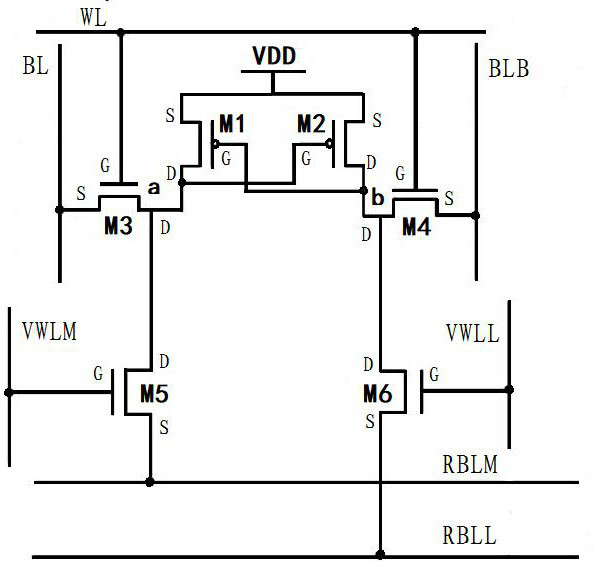
[0052] Such as figure 2 Shown is a schematic structural diagram of a 6T SRAM computing device 1 in Embodiment 1 of the present invention. The storage and calculation device 1 includes a storage part and a calculation part. Among them, the storage part is used to store the input weight; the calculation part is used to perform weighted calculation on the weight and the input data;
[0053] The storage part includes 4 transistors: transistor M1, transistor M2, transistor M3 and transistor M4; the calculation part includes 2 transistors: transistor M5 and transistor M6. G in the figure represents the gate of the transistor, S represents the source of the transistor, and D represents the drain of the transistor.
[0054] The source of the transistor M3 is connected to the bit line BL as the first weight input terminal of the storage and calculation device 1; the source of the transistor M4 is connected to the bit line BLB as the second weight input terminal of the storage and ca...
Embodiment 2
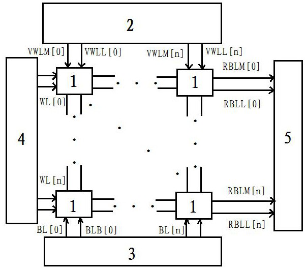
[0071] Such as image 3 It is a schematic structural diagram of a 6T SRAM storage and computing system in Embodiment 2 of the present invention.
[0072] Specifically, on the basis of the 6T SRAM computing device 1, an input driver 2, a column decoding and bit line driving module 3, a row decoder 4, and a weighted bitwise multiply-accumulate output module 5 are added.
[0073] in,
[0074] The input driver 2 is connected with the gate of the transistor M5 in the storage and calculation device 1 through the input line VWLM, and is used to input the first bit of data in the transistor M5; it is connected with the gate of the transistor M6 through the input line VWLL, and is used for inputting the first bit of the data to the transistor M6. The second bit of the input data in M6;
[0075] The column decoding and bit line driving module 3 is connected to the source of the transistor M3 in the storage device 1 through the bit line BL, and is used to input the first weight to the ...
PUM
 Abstract
Description
Claims
Application Information


