Modified Xilinx FPGA power-on reset circuit
An improved technology of power-on reset, which is applied in the field of power-on reset circuit system, can solve the problems of different time delays of reset signal lines, time errors of power-on reset, and inaccurateness, etc., and achieve improved signal quality, accurate reset time, The effect of improving stability
- Summary
- Abstract
- Description
- Claims
- Application Information
AI Technical Summary
Problems solved by technology
Method used
Image

Examples
Embodiment Construction
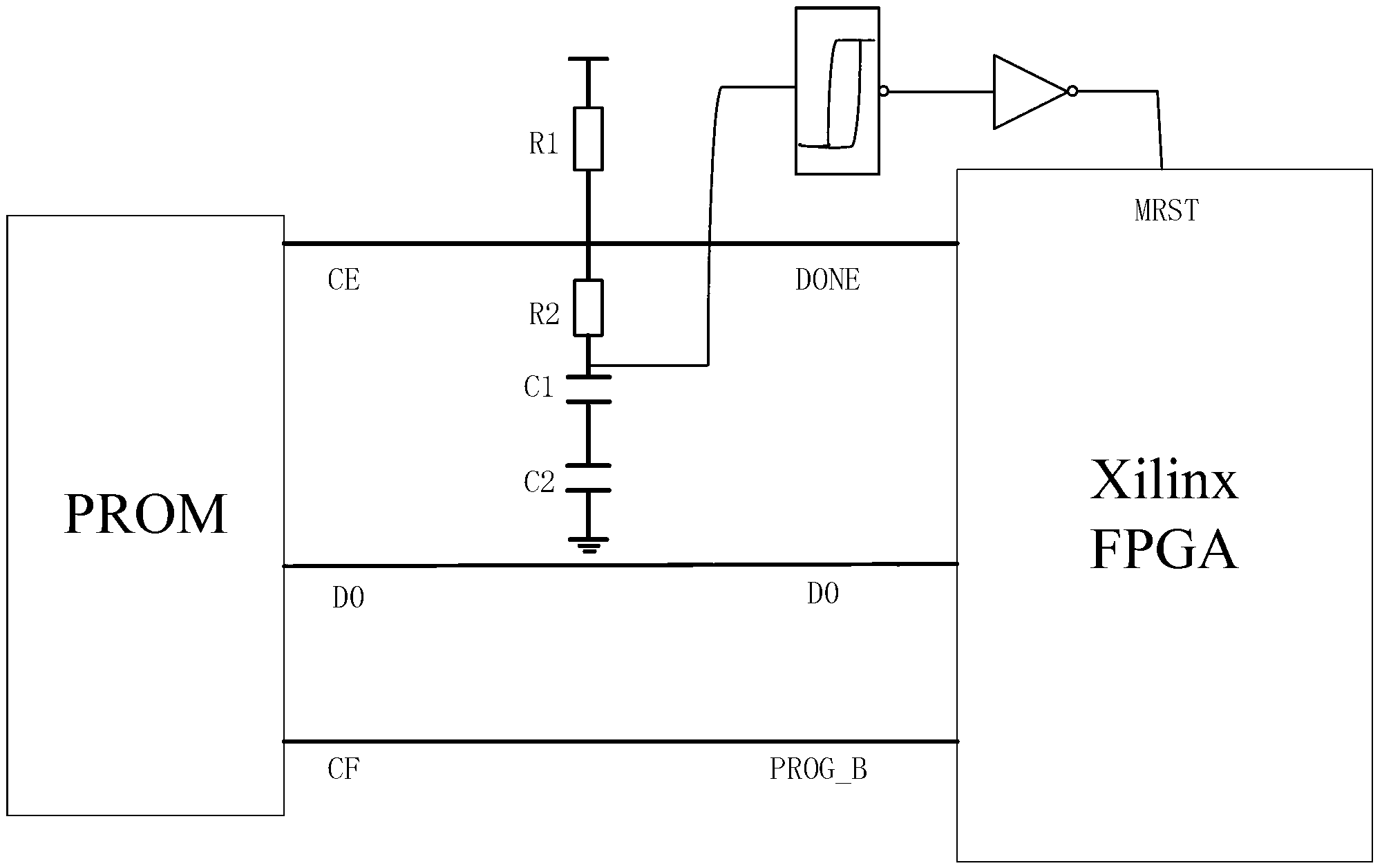
[0023] image 3 Shown is the schematic diagram of the FPGA power-on reset circuit of the present invention, wherein the PROM uses the XCF16P of Xilinx Company, and the FPGA uses the Virtex-II series XC2V3000 of Xilinx Company. In the system design, the circuit design takes the DONE signal as the global reset input of the software after passing the RC delay through the Schmitt trigger and the inverter, that is, the MRST signal in the summary diagram. The hardware design mainly considers the requirement that the power-on reset delay is greater than 10ms. The resistance value of the RC delay reset circuit can be selected as 4.7K ohms. In order to improve the withstand voltage performance of the capacitor, two 22uF tantalum capacitors are used in series, and the positive For a Schmitt trigger with a threshold voltage of 3v, the rise time of the reset signal (0-3v time) can be calculated by the RC delay formula, such as formula (1), which is about 100ms. In this way, the low-to-hi...
PUM
 Abstract
Description
Claims
Application Information