Wafer pre-locating device based on machine vision and method thereof

A pre-positioning device and machine vision technology, applied in semiconductor/solid-state device manufacturing, electrical components, circuits, etc., can solve the problems of polluted wafers, expensive, complex cost of optical alignment structures, etc., and achieve simple system structure and low cost Effect

Inactive Publication Date: 2013-07-24
SHENYANG INST OF AUTOMATION - CHINESE ACAD OF SCI
View PDF2 Cites 39 Cited by
  • Summary
  • Abstract
  • Description
  • Claims
  • Application Information

AI Technical Summary

Problems solved by technology

If mechanical positioning is used, it will inevitably damage and contaminate the wafer, and the existing optical alignment structure is c

Method used


Image

  • Wafer pre-locating device based on machine vision and method thereof
  • Wafer pre-locating device based on machine vision and method thereof
  • Wafer pre-locating device based on machine vision and method thereof

Examples


Embodiment Construction

[0029] The present invention will be further described in detail below in conjunction with the accompanying drawings and embodiments.

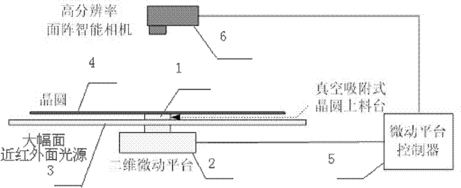
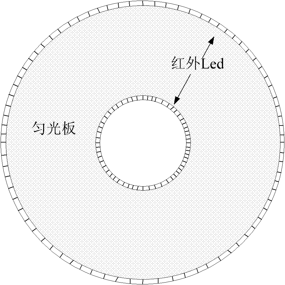
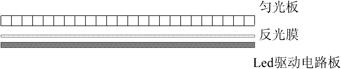
[0030] The wafer pre-positioning device based on machine vision proposed by the present invention includes a vacuum adsorption wafer loading platform, a high-resolution area array smart camera, a large-format infrared light source, and a high-precision two-dimensional micro-motion platform. The pre-positioning method is to first use a high-resolution area array smart camera as a sensor to image the wafer on the loading table, then extract the edge of the wafer through a high-precision edge detection algorithm, and use the least squares algorithm to fit the coordinates of its center, and finally The difference between the current position coordinates of the center of the circle and the reference position coordinates is used as feedback to drive the two-dimensional micro-motion platform, and the wafer position is adjusted to reach the reference p...


PUM


Abstract

The invention relates to a wafer pre-locating device based on machine vision and a method thereof. The device comprises a vacuum-absorbing type wafer feeding table, an image collecting and processing unit, a large-format infrared face area light source and a two-dimension micro-motion platform system. The method comprises the steps of feeding wafers, collecting images of the wafers; extracting edges; fitting circle centers of the wafers; and adjusting positions of the wafers. The device and the method avoid damage to the edges of the wafers, and have the advantages of being free of any adjustment and capable of meeting requirements for accurate location of the wafers. Meanwhile, the device is simple in structure, low in cost, and capable of meeting requirements of manufacture of IC equipment for pre-location of the wafers.

Description

technical field [0001] The invention relates to the technical field of machine vision, in particular to a wafer pre-positioning device and method in the field of IC manufacturing. Background technique [0002] The wafer pre-positioning device is a core component in the IC manufacturing process. Its function is to adjust the position of the wafer before the wafer is transferred to the processing table to ensure that the center of the wafer is within a limited range. In some IC manufacturing equipment, such as lithography machines, not only the precise positioning of the wafer but also the pre-alignment of the wafer are required, even if the center of the wafer is within the limited range, the notch (or edge trimming) of the silicon wafer ) is also within a certain range of angles. The accuracy of the pre-positioning / alignment system directly affects the efficiency and yield of the entire IC manufacturing system, and has become a key component of many IC equipment. [0003] ...

Claims


Application Information

Patent Timeline
IPC IPC(8): H01L21/68
Inventor 吴清潇欧锦军朱枫郝颖明付双飞苗锡奎
Owner SHENYANG INST OF AUTOMATION - CHINESE ACAD OF SCI
Why Eureka
Try Eureka