LED (light emitting diode) display screen and manufacture method thereof

A technology of LED display and manufacturing method, which is applied in semiconductor/solid-state device manufacturing, electrical components, circuits, etc., and can solve the problems of LED display pixel density and definition that cannot achieve higher definition, uneven current distribution, etc.

Inactive Publication Date: 2013-07-24
ENRAYTEK OPTOELECTRONICS
View PDF2 Cites 12 Cited by
  • Summary
  • Abstract
  • Description
  • Claims
  • Application Information

AI Technical Summary

Problems solved by technology

[0006] The invention provides an LED display screen and a manufacturing method thereof to solve the problem that the pixel density and definition of the LED display screen cannot achieve higher definition display
[0008] Another object of the present invention is to solve the problem of uneven current distribution in the chip of the LED display

Method used


Image

  • LED (light emitting diode) display screen and manufacture method thereof
  • LED (light emitting diode) display screen and manufacture method thereof
  • LED (light emitting diode) display screen and manufacture method thereof

Examples


Embodiment Construction

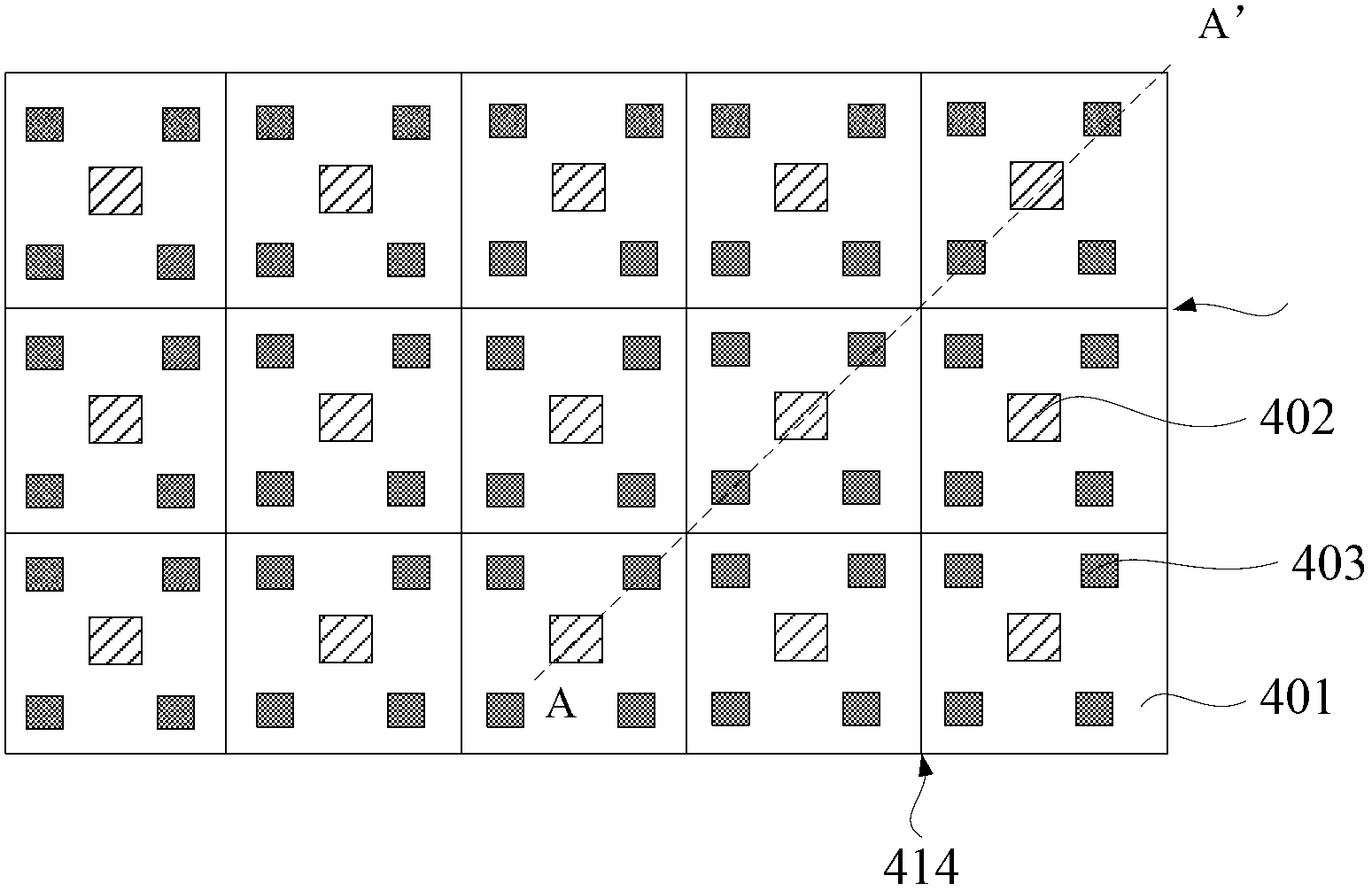
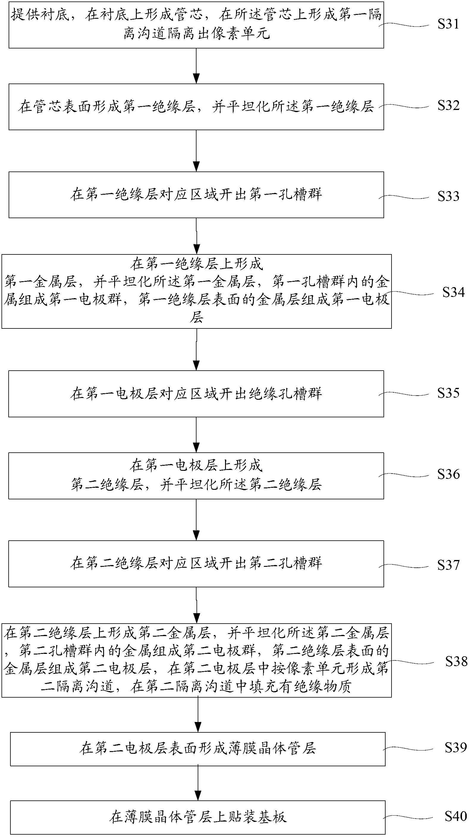
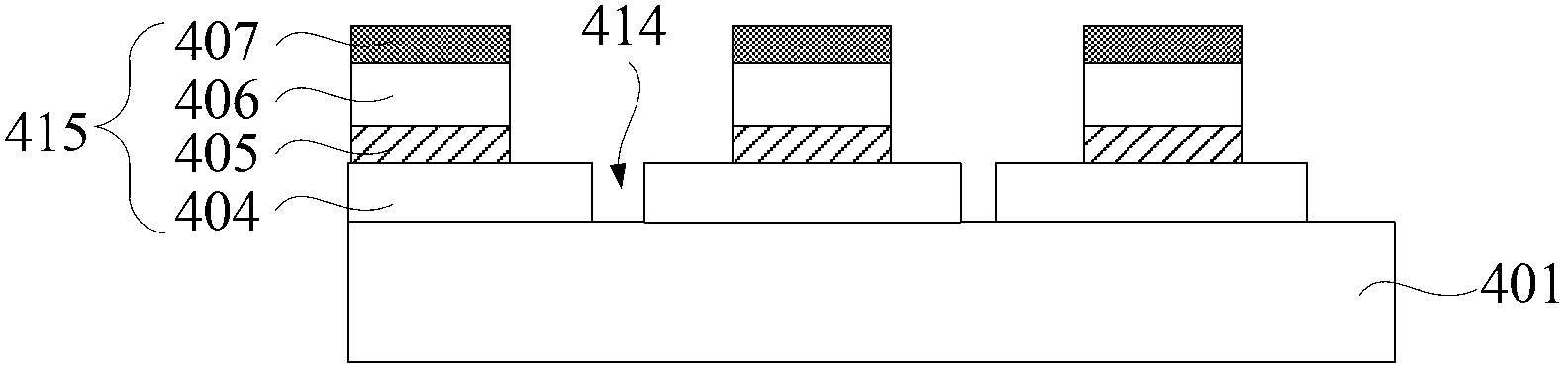
[0035] It has been mentioned in the background technology that since the pixel module of the existing LED display is integrated and packaged by many pixel units, there is inevitably a large gap between the pixel units, which affects the pixel density and Clarity makes a huge difference. At the same time, the traditional flip-chip manufacturing method increases the process steps and difficulty, and limits the further development of LED display screens in thickness and size.

[0036] To this end, the present invention provides an LED display screen and a manufacturing method thereof. The pixel module of the LED display is a single LED chip, and the LED chip includes: a substrate, a tube core formed on the substrate, and a An electrode on the die and in contact with the corresponding area of ​​the die, the electrode includes a first electrode group and a second electrode group, a first electrode layer is formed on the first electrode group, and a first electrode layer is formed o...


PUM


Abstract

The invention discloses an LED (light emitting diode) display screen and a manufacture method thereof. A pixel module of the LED display screen is a single LED chip, and a gap between every two pixels can be effectively controlled, thus the definition of the LED display screen is improved. Meanwhile, the traditional upside-down mounting chip process is optimized to the process that after an electrode group is generated, structures of an electrode layer, an insulation layer and the like are generated, so that the thickness of a chip is effectively controlled, the traditional arrangement of a pair of electrodes is divided into a first electrode group and a second electrode group which are distributed in the corresponding area of a tube core, by adopting the structure, sufficient current expansion can be obtained, current is enabled to be uniformly distributed, a device is enabled to obtain excellent luminescent efficiency and uniform glaring rate, and the requirement that a chip size is further increased can be met.

Description

technical field [0001] The invention relates to the technical field of LED manufacturing, in particular to an LED display screen and a manufacturing method thereof. Background technique [0002] Light Emitting Diode (LED, Light Emitting Diode) is a semiconductor solid-state light-emitting device that uses a semiconductor PN junction as a light-emitting material to convert electricity into light. When a forward voltage is applied to both ends of the semiconductor PN junction, the electrons and holes injected into the PN junction recombine, and the excess energy is released in the form of photons. LED has the advantages of long life and low power consumption. With the maturity of technology, the application fields of LED are becoming more and more diversified. Among them, the manufacturing process of LED display field is also becoming more and more mature. Bead arrays form single-color displays to colorful and full-color displays composed of LED chips and matrix blocks. LED d...

Claims


Application Information

Patent Timeline
Patent Type & Authority Applications(China)
IPC IPC(8): H01L21/82H01L21/84H01L21/50H01L33/38
Inventor 毕少强
Owner ENRAYTEK OPTOELECTRONICS
Why Eureka
Try Eureka