Plasma processing device

A plasma and processing device technology, which is applied in the field of plasma processing devices, can solve the problems of intensified plasma bombardment of the focus ring, damage to the focus ring, etc., and achieve the effect of prolonging the service life and uniform treatment process

Active Publication Date: 2013-07-31
ADVANCED MICRO FAB EQUIP INC CHINA
View PDF7 Cites 33 Cited by
  • Summary
  • Abstract
  • Description
  • Claims
  • Application Information

AI Technical Summary

Problems solved by technology

However, for components with conductive materials in the reaction chamber, such as the focus ring, this superimposed vertical RF electric field will intensify the bombardment of the plasma on the focus ring, which may cause damage to the focus ring

Method used


Image

  • Plasma processing device
  • Plasma processing device
  • Plasma processing device

Examples


Embodiment 1

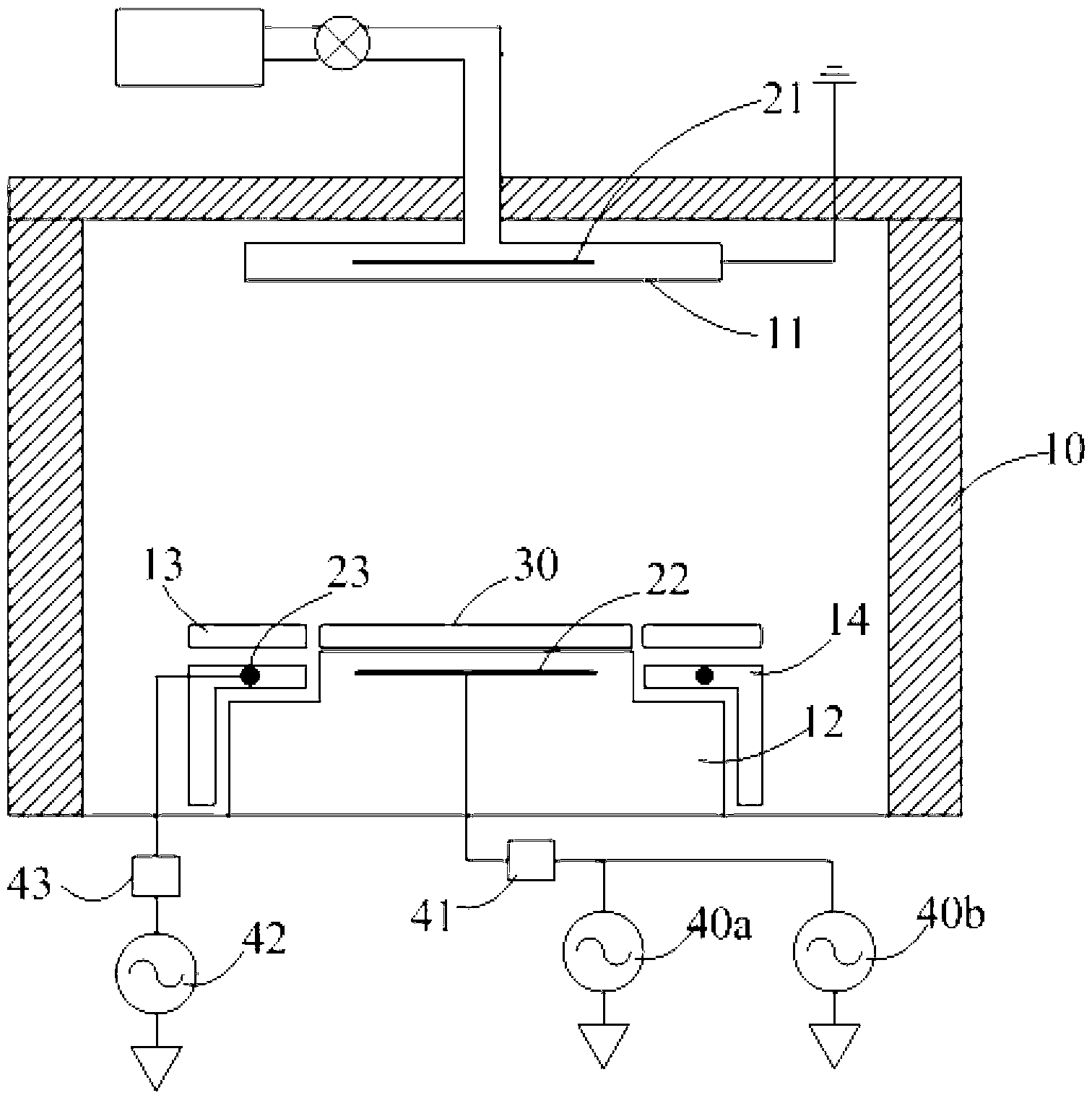
[0031] See figure 2 , which is a schematic structural diagram of the plasma processing chamber in this embodiment. The plasma processing device comprises a reaction chamber 10, wherein a reaction gas is introduced; the top of the reaction chamber 10 is provided with a reaction gas shower head 11, and the reaction gas shower head 11 includes a flat upper electrode 21, and the upper electrode 21 is grounded. ; The bottom of the reaction chamber 10 is provided with an electrostatic chuck 12 for clamping a substrate 30, which can be a semiconductor substrate to be etched or processed or a glass plate to be processed into a flat panel display. A flat-plate lower electrode 22 parallel to the upper electrode 21 is disposed in the electrostatic chuck 12 . The lower electrode 22 is connected to the first radio frequency source 40a and the second radio frequency source 40b through the first radio frequency matching device 41 . The first radio frequency source 40a and the second radio...

Embodiment 2

[0037] Figure 4 is a schematic structural view of another embodiment of the plasma processing device provided by the present invention, Figure 4 The illustrated embodiments can be provided independently or in combination with the above-described embodiments.

[0038] The difference between this embodiment and Embodiment 1 is that the reaction chamber in this embodiment includes a plasma confinement assembly 15, which includes a plurality of concentric rings 15a stacked on each other in the vertical direction and arranged parallel to each other at intervals. These concentric rings 15a Surrounding the area above the electrostatic chuck, that is, the area between the upper electrode 21 and the lower electrode 22 , this area can be considered as a reaction area P where plasma is formed and the substrate 30 is processed. There is a gap between the adjacent concentric rings 15a. When the substrate 30 is treated with plasma, the treated reaction gas can be discharged out of the re...


PUM


Abstract

The invention discloses a plasma processing device which comprises a reaction cavity, a first radio-frequency power source and a second radio-frequency power source, wherein the reaction cavity comprises an upper electrode and a lower electrode which are arranged in parallel, an annular insulator, and opening metal ring electrodes; the upper electrode is arranged in a gas spray header; the lower electrode is arranged in a static clamping chuck; the first radio-frequency power source is used for forming a perpendicular radio-frequency electric field between the upper and lower electrodes to generate plasma; the second radio-frequency power source is used for adjusting energy of the plasma; the annular insulator surrounds the static clamping chuck and / or an area above the static clamping chuck; the opening metal ring electrodes are wound by wires, and embedded into the annular insulator; and a radio-frequency current is supplied in the metal ring electrodes to generate a horizontal induction electric field. The plasma processing device can improve the uniformity of density distribution of the plasma in the reaction cavity effectively.

Description

technical field [0001] The invention relates to semiconductor processing equipment, in particular to a plasma processing device. Background technique [0002] In recent years, with the development of semiconductor manufacturing processes, the requirements for the integration and performance of components are getting higher and higher, and plasma technology (Plasma Technology) has been widely used. Plasma technology introduces a reactive gas and electron flow into the reaction chamber of the plasma processing device, uses a radio frequency electric field to accelerate the electrons, and collides with the reactive gas to ionize the reactive gas and generate plasma. The generated plasma can be used Used in various semiconductor manufacturing processes, such as deposition processes (such as chemical vapor deposition), etching processes (such as dry etching), etc. [0003] Plasma processing often employs capacitively coupled plasma processing devices to generate plasma. figure ...

Claims


Application Information

Patent Timeline
Patent Type & Authority Applications(China)
IPC IPC(8): H01J37/32
Inventor 倪图强梁洁罗伟义
Owner ADVANCED MICRO FAB EQUIP INC CHINA
Why Eureka
Try Eureka