Plasma processing device

A plasma and processing device technology, which is applied in the field of plasma processing devices, can solve the problems of fast etching or processing speed in the middle of the substrate, uneven plasma processing technology, and unsatisfactory plasma density uniformity, etc., and achieves a simple structure , plasma treatment process is uniform, the effect of system stability

Active Publication Date: 2014-12-17
ADVANCED MICRO FAB EQUIP INC CHINA
View PDF5 Cites 13 Cited by
  • Summary
  • Abstract
  • Description
  • Claims
  • Application Information

AI Technical Summary

Problems solved by technology

[0004] However, in practical applications, the uniformity of the plasma density generated by the capacitively coupled plasma processing device is not ideal.
Due to the structural characteristics of capacitive coupling, there is a difference in the electric field strength between the middle region and the edge region in the reaction chamber, and the density of the generated plasma has a characteristic distribution that the middle region is higher than the edge region, and due to the plasma processing rate of the substrate In connection with this plasma density, it will eventually lead to inhomogeneous plasma treatment process: for example, fast etching or processing rate in the middle of the substrate, slow etching or processing rate at the edge

Method used


Image

  • Plasma processing device
  • Plasma processing device
  • Plasma processing device

Examples


Embodiment Construction

[0025] The specific embodiments of the present invention will be described below in conjunction with the accompanying drawings.

[0026] It should be understood that the plasma processing device in the present invention can be a device such as plasma etching, plasma physical vapor deposition, plasma chemical vapor deposition, plasma surface cleaning, etc., and the plasma processing device is only exemplary. Fewer or more constituent elements may be included, or the arrangement of the constituent elements may be the same as or different from that shown in the drawings.

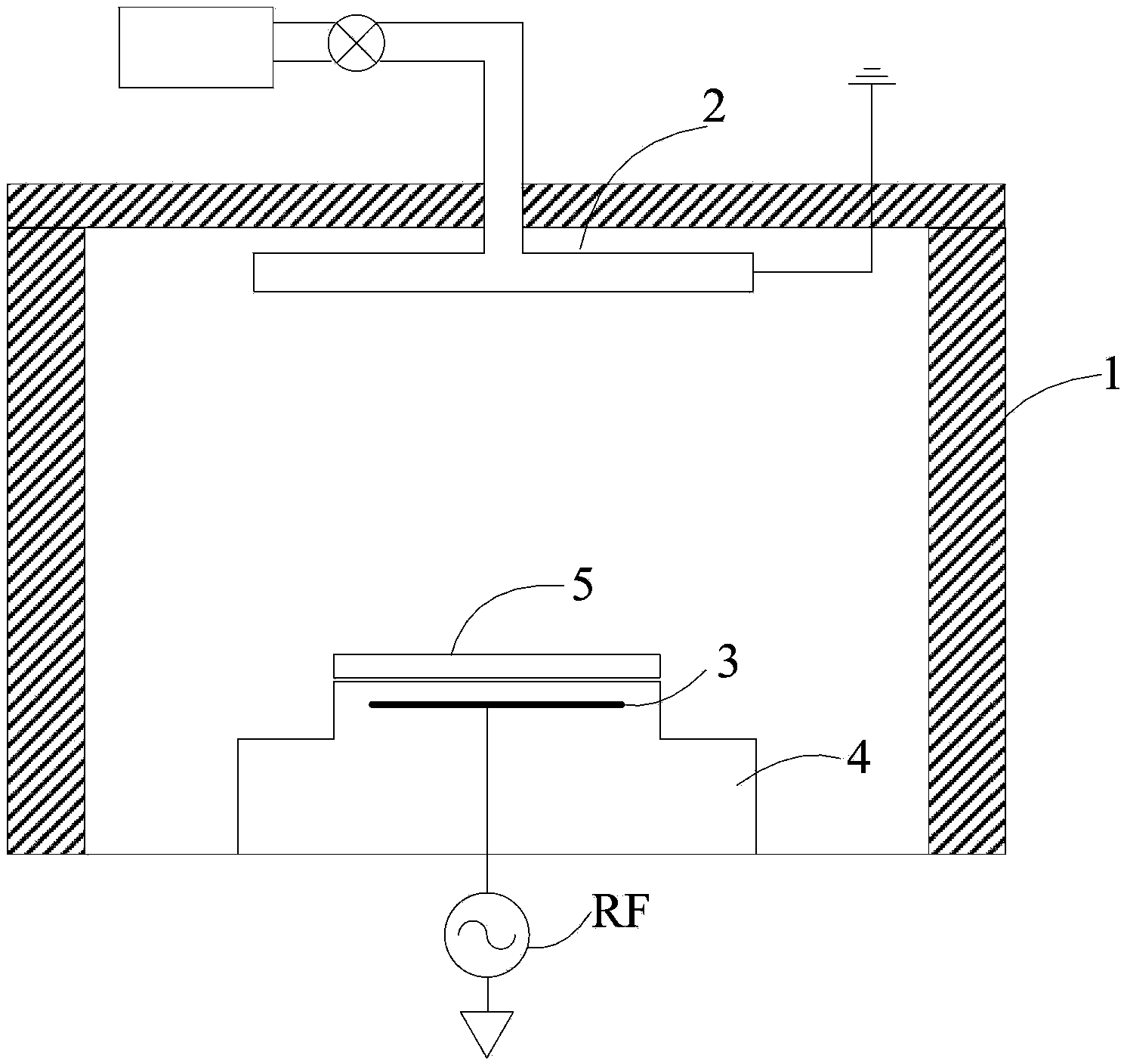
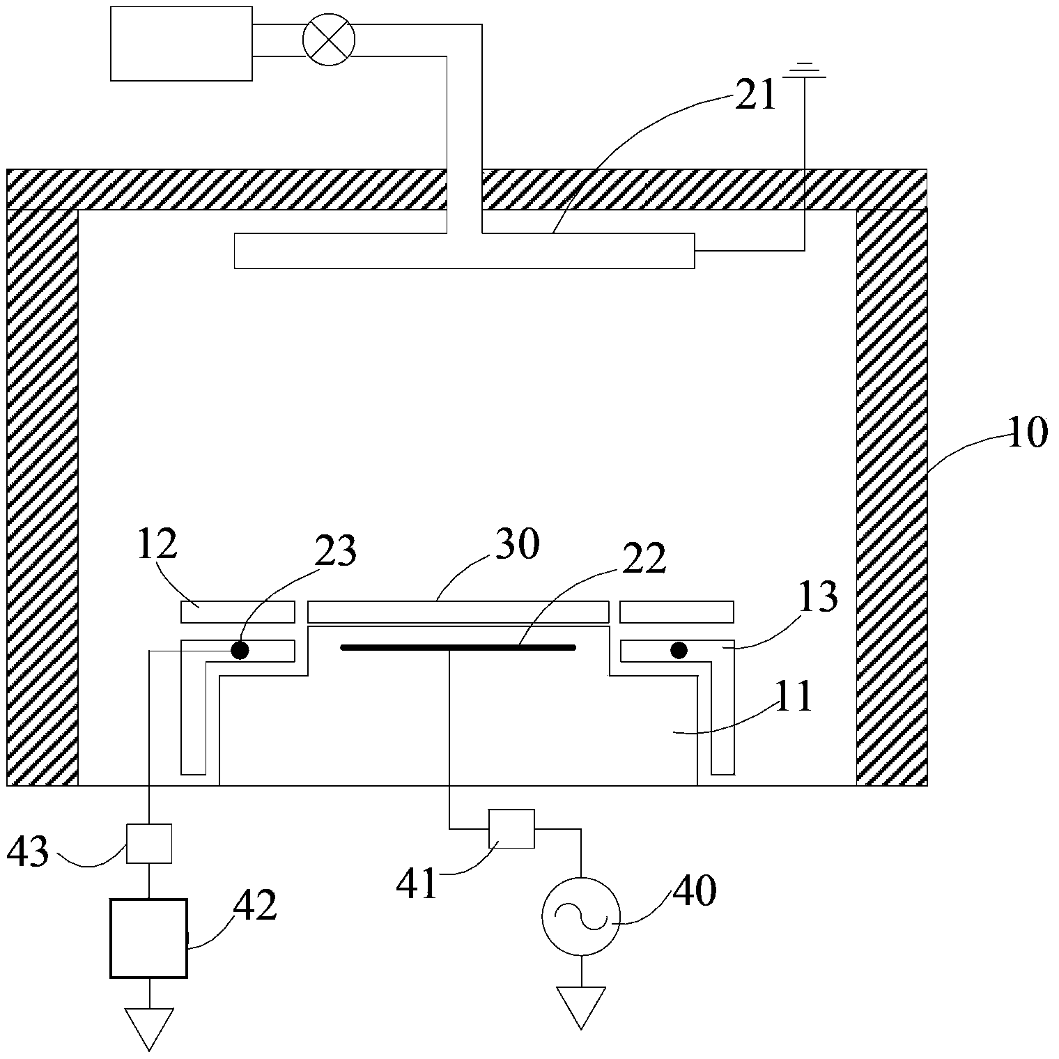
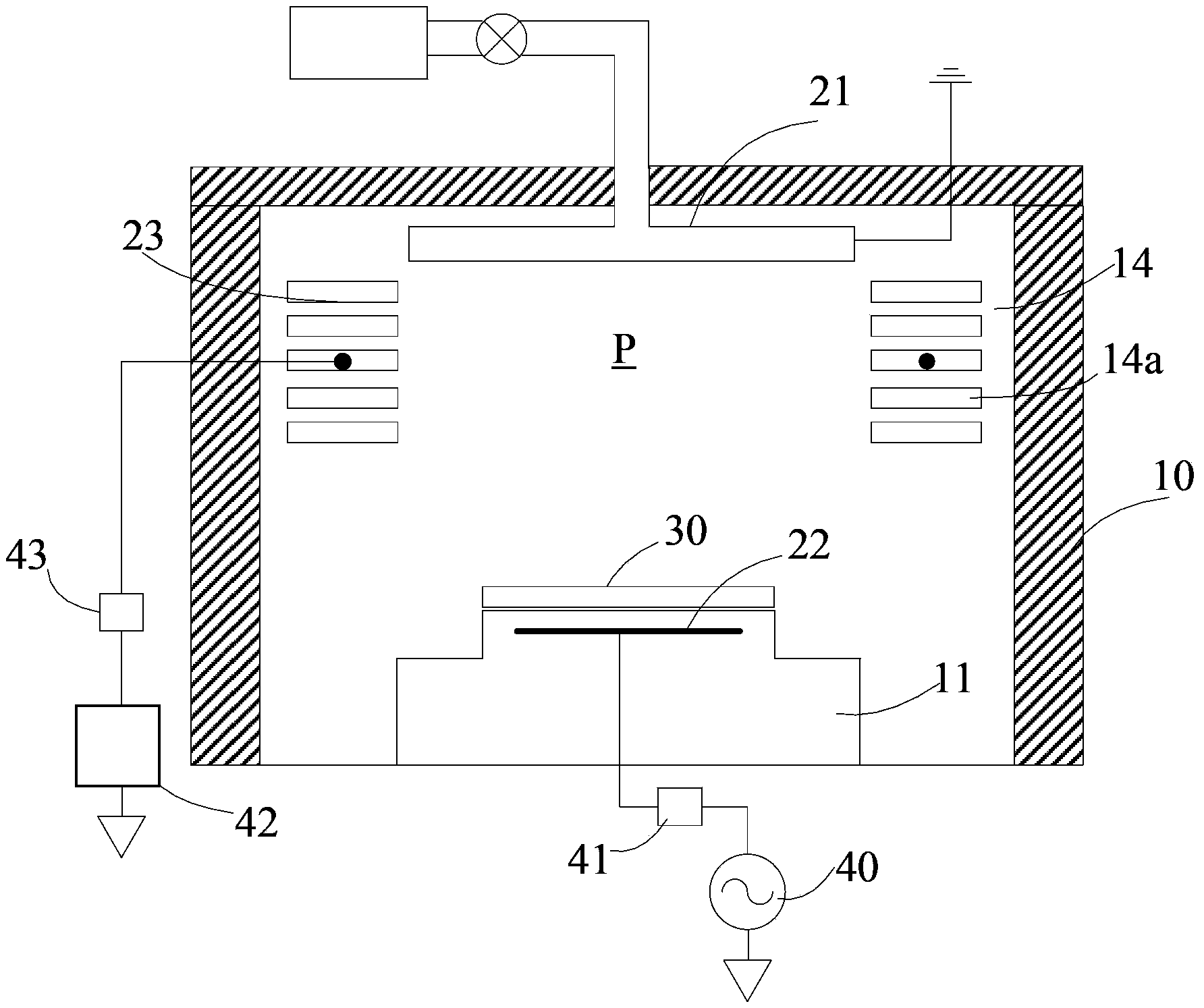
[0027] See figure 2 , which is a schematic structural diagram of the plasma processing chamber in this embodiment. The plasma processing device comprises a reaction chamber 10, wherein a reaction gas is introduced; the top of the reaction chamber 10 is provided with a reaction gas shower head, and the reaction gas shower head includes a flat upper electrode 21, and the upper electrode 21 is grounded; the bott...


PUM


Abstract

The invention provides a plasma processing device. The plasma processing device comprises a reaction cavity, an upper electrode and a lower electrode which are parallel to each other are arranged in the reaction cavity, the lower electrode is arranged in a base, the base comprises a static chuck, and a substrate is arranged on the static chuck for processing. The plasma processing device is characterized by also comprising an annular insulator, a first electrode, a first radio frequency power source and a pulse DC power supply, wherein the annular insulator encircles the static chuck and / or a region above the static chuck, the first electrode is embedded in the annular insulator, the first radio frequency power source is connected with the lower electrode via a first radio frequency matcher and used for providing radio frequency power to form a radio frequency electric field in a vertical direction between the upper electrode and the lower electrode so as to generate plasma, and the pulse DC power supply is connected to the first electrode. Through adoption of the plasma processing device, the uniformity of substrate processing can be improved.

Description

technical field [0001] The invention relates to the field of semiconductor manufacturing, in particular to a plasma processing device. Background technique [0002] In recent years, with the development of semiconductor manufacturing processes, the requirements for the integration and performance of components are getting higher and higher, and plasma technology (Plasma Technology) has been widely used. Plasma technology introduces a reactive gas and electron flow into the reaction chamber of the plasma processing device, uses a radio frequency electric field to accelerate the electrons, and collides with the reactive gas to ionize the reactive gas and generate plasma. The generated plasma can be used Used in various semiconductor manufacturing processes, such as deposition processes (such as chemical vapor deposition), etching processes (such as dry etching), etc. [0003] Plasma processing often employs capacitively coupled plasma processing devices to generate plasma. f...

Claims


Application Information

Patent Timeline
Patent Type & Authority Applications(China)
IPC IPC(8): H01J37/32
Inventor 梁洁叶如彬
Owner ADVANCED MICRO FAB EQUIP INC CHINA
Why Eureka
Try Eureka