Polycrystalline silicon forming method, TFT (thin film transistor) array substrate manufacturing method and display device

An array substrate, polysilicon technology, applied in semiconductor/solid-state device manufacturing, transistors, instruments, etc., can solve the problems of easy early turn-on and hump, and achieve the effect of avoiding hump phenomenon

Active Publication Date: 2013-08-28
SHANGHAI TIANMA MICRO ELECTRONICS CO LTD
View PDF2 Cites 26 Cited by
  • Summary
  • Abstract
  • Description
  • Claims
  • Application Information

AI Technical Summary

Problems solved by technology

[0005] The purpose of the present invention is to provide a TFT array substrate and its manufacturing method, so as to solve the problem of the existing TFT array substrate, the TFT is easy to be turned on early at the edge of the channel, and the hump phenomenon is formed

Method used


Image

  • Polycrystalline silicon forming method, TFT (thin film transistor) array substrate manufacturing method and display device
  • Polycrystalline silicon forming method, TFT (thin film transistor) array substrate manufacturing method and display device
  • Polycrystalline silicon forming method, TFT (thin film transistor) array substrate manufacturing method and display device

Examples


Embodiment Construction

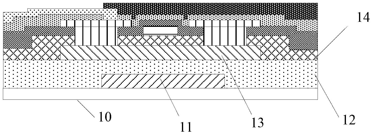
[0028] The invention provides a method for forming polysilicon in a TFT array substrate. In the method, a special step structure is formed at the position of the light-shielding layer corresponding to the TFT channel region, and the crystallization of the subsequently formed polysilicon layer is not saturated at the corresponding position, that is, the obtained The crystal failure at the edge of the TFT channel avoids hump phenomenon.

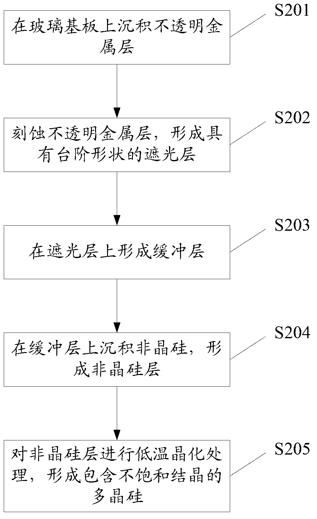
[0029] Embodiment 1 of the present invention provides a method for forming polysilicon in a TFT array substrate. The schematic flow diagram of the method is shown in figure 2 shown.

[0030] Step S201 : Depositing an opaque metal layer on the glass substrate 10 .

[0031] Specifically, firstly, the glass substrate 10 is cleaned through an initial cleaning process, and an opaque metal of a certain thickness is deposited on the cleaned glass substrate 10 by magnetron sputtering (PVD) method.

[0032] Step S202: Etching the opaque metal layer i...


PUM


Abstract

The invention discloses a polycrystalline silicon forming method, a TFT (thin film transistor) array manufacturing method and a display device, which solves the problems in the prior art that the TFT on the edge of a ditch is easy to start in advance and a hump phenomenon is formed. A step-shaped light shielding layer is formed on a position for performing the TFT, the position of the step shape corresponds to the edge of the TFT ditch, the light shielding layer is provided with a buffering layer and a noncrystalline silicon layer, which are respectively in a consistent step shape, the noncrystalline silicon layer is crystallized at a low temperature to form polycrystalline silicon containing unstaturated crystal, so that the crystallization of the polycrystalline silicon on the edge of the ditch loses the effectiveness, the current of the TFT device on the edge of the ditch is reduced, the situation that the TFT on the edge of the ditch is early started can be avoided, and the hump phenomenon can be avoided.

Description

technical field [0001] The invention relates to the field of liquid crystal display manufacture, in particular to a method for forming polysilicon, a method for manufacturing a TFT array substrate and a display device. Background technique [0002] The display panel made of low temperature polysilicon technology (Low Temperature Poly-silicon, LTPS) can reduce the power consumption of the display screen, and the LTPS TFT (Thin Film Transistor, thin film transistor) display panel has high resolution, fast response, high With advantages such as brightness and high aperture ratio, LTPS TFT display panels are more and more widely used. [0003] In the existing LTPS TFT array substrate manufacturing process, it is first necessary to deposit an opaque metal layer on the glass substrate 10, etch the opaque metal layer to form the light shielding layer 11 that shields the light from the backlight from irradiating the TFT channel, and the light shielding layer A buffer layer 12 is fo...

Claims


Application Information

Patent Timeline
Patent Type & Authority Applications(China)
IPC IPC(8): H01L21/20H01L21/77H01L29/786G02F1/1362G02F1/1368
CPCH01L27/1288H01L29/78633H01L29/78696
Inventor 彭涛
Owner SHANGHAI TIANMA MICRO ELECTRONICS CO LTD
Why Eureka
Try Eureka