Array substrate and manufacturing method thereof and display panel

A technology of array substrates and substrate substrates, which is applied in semiconductor/solid-state device manufacturing, optics, instruments, etc., can solve problems such as poor display, achieve enhanced display effects, improve picture display quality, and improve user experience

Inactive Publication Date: 2013-09-11
BOE TECH GRP CO LTD +1
View PDF3 Cites 10 Cited by
  • Summary
  • Abstract
  • Description
  • Claims
  • Application Information

AI Technical Summary

Problems solved by technology

[0007] Embodiments of the present invention provide an array substrate, a manufacturing method thereof, and a display panel, which are used to solve the problem of bad display caused by broken data lines and improve the picture quality of the liquid crystal panel

Method used


Image

  • Array substrate and manufacturing method thereof and display panel
  • Array substrate and manufacturing method thereof and display panel
  • Array substrate and manufacturing method thereof and display panel

Examples


preparation example Construction

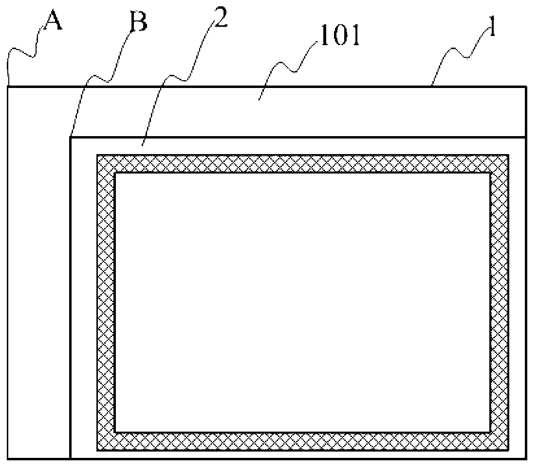
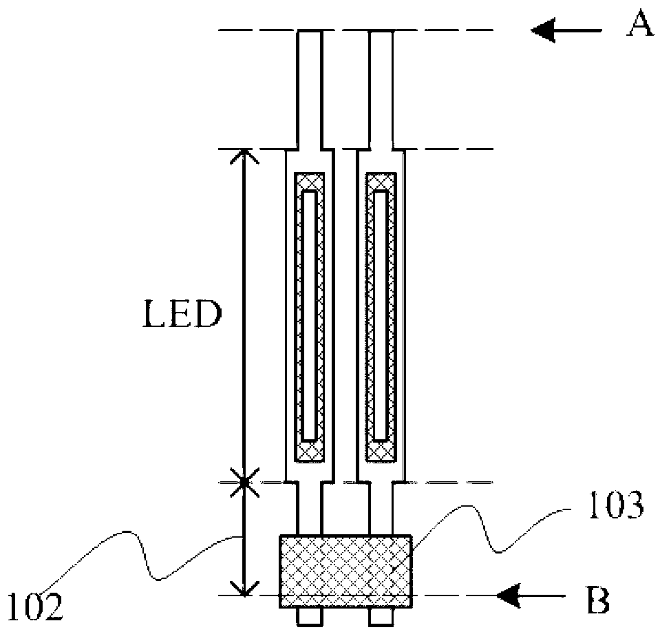
[0048] A method for preparing an array substrate provided by an embodiment of the present invention includes: forming a gate scanning line on a base substrate, forming a gate insulating layer above the gate scanning line, forming an active layer above the gate insulating layer, and forming an active layer on the active layer. Fabricate a data line above the data line, fabricate a passivation layer above the data line, and fabricate a pixel electrode on the passivation layer; the method also includes:

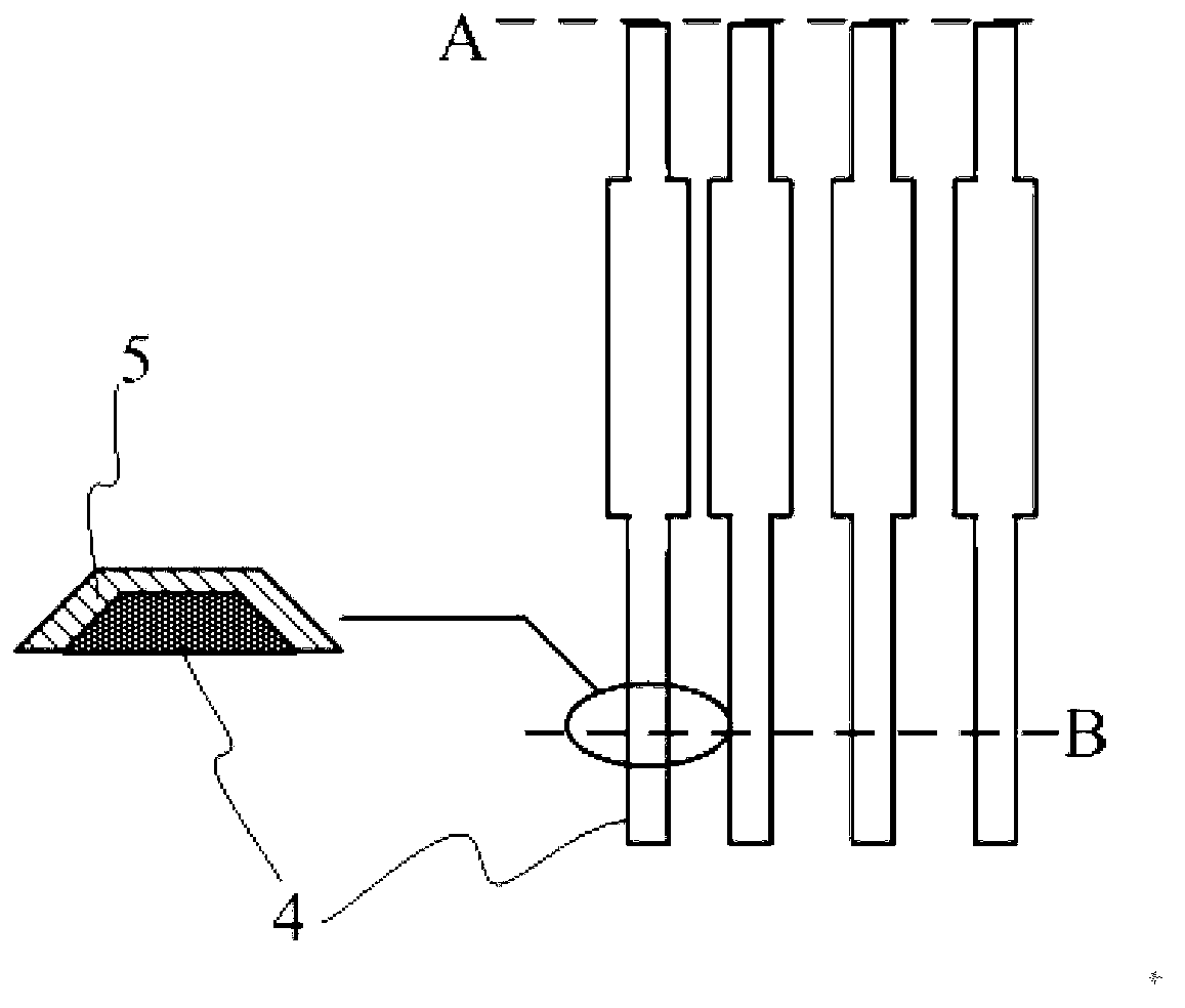
[0049] Make a connection line corresponding to each data line above the base substrate, and the connection line is connected to the data line through the bridge structure of the LED area and the area below the cutting line of the box substrate;

[0050] Fabricate a bridging structure above the passivation layer, and the bridging structure is arranged on the same layer as the pixel electrode.

[0051] Preferably, the method further includes: forming a first-type via hole penetrat...


PUM


Abstract

The invention provides an array substrate and a manufacturing method thereof and a display panel, aiming to solve the problem of bad displaying in the prior art due to data line disconnection and further improving display effect of a liquid crystal display device. The array substrate comprises a lining substrate, a grid scanning line, a grid insulating layer, an active layer, data lines, a passivation layer, a pixel electrode, connecting lines and bridge connection structures. The connecting lines and the bridge connection structures correspond with each data line. The bridge connection structures are disposed above the passivation layer and arranged on the same layer with the pixel electrode. Each of the connecting lines is disposed above the lining substrate, and is connected with the data lines through the bridge connection structures in an LED (light-emitting diode) area and an area below combined substrate cutting lines.

Description

technical field [0001] The invention relates to the technical field of liquid crystal display, in particular to an array substrate, a manufacturing method thereof, and a display panel. Background technique [0002] With the development of thin film transistor liquid crystal display technology and the progress of industrial technology, liquid crystal display technology has replaced cathode ray tube technology and become the mainstream technology in the field of daily display. Due to the reduction in production cost of liquid crystal display devices and the increasingly perfect manufacturing process, its own advantages have become ideal display devices in the minds of the market and consumers. At present, the stereoscopic display technology is rising day by day in the market, so it is also necessary to solve the technical shortcomings of the stereoscopic display technology and improve the image quality (such as reducing color cast, reducing bright spots, bright lines, reducing...

Claims


Application Information

Patent Timeline
IPC IPC(8): G02F1/1362G02F1/1368H01L21/77
CPCH01L27/124G02F1/133351G02F1/13458H01L27/1248G02F1/136259H01L27/1244G02F1/136263G02F1/136286G02F1/1368
Inventor 陈曦冯玉春袁剑峰王琳琳
Owner BOE TECH GRP CO LTD
Why Eureka
Try Eureka