Electronic device encapsulated with welding end ring and electronic equipment provided with electronic device

A technology for electronic devices and solder terminals, applied in the field of electronic equipment, can solve the problems of early failure, cracks in solder joints, poor product reliability, etc., and achieve the effect of reducing application concentration, large scalable paths, and not easy to fail.

Active Publication Date: 2013-09-18
HUAWEI TECH CO LTD
View PDF5 Cites 1 Cited by
  • Summary
  • Abstract
  • Description
  • Claims
  • Application Information

AI Technical Summary

Problems solved by technology

When this type of device in the prior art is soldered on the PCB, the height of the solder paste climbing along the soldering end is small, resulting in a small amount of tin at the soldering end
Since the body is ceramic, it does not match the CTE (Coefficient of Thermal Expansion, coefficient of thermal expansion) of the PCB, and the small amount of tin at the soldering end does not play a good role in reducing the mismatch of CTE, so in long-term operation , the solder joints are prone to cracks, which cannot meet the long-term reliability requirements of the product
Moreover, the stress on the solder joint at the soldering end is high and cracks are likely to appear, and the crackable expansion path is small, which is prone to early failure and poor product reliability.

Method used


Image

  • Electronic device encapsulated with welding end ring and electronic equipment provided with electronic device
  • Electronic device encapsulated with welding end ring and electronic equipment provided with electronic device
  • Electronic device encapsulated with welding end ring and electronic equipment provided with electronic device

Examples


Embodiment 1

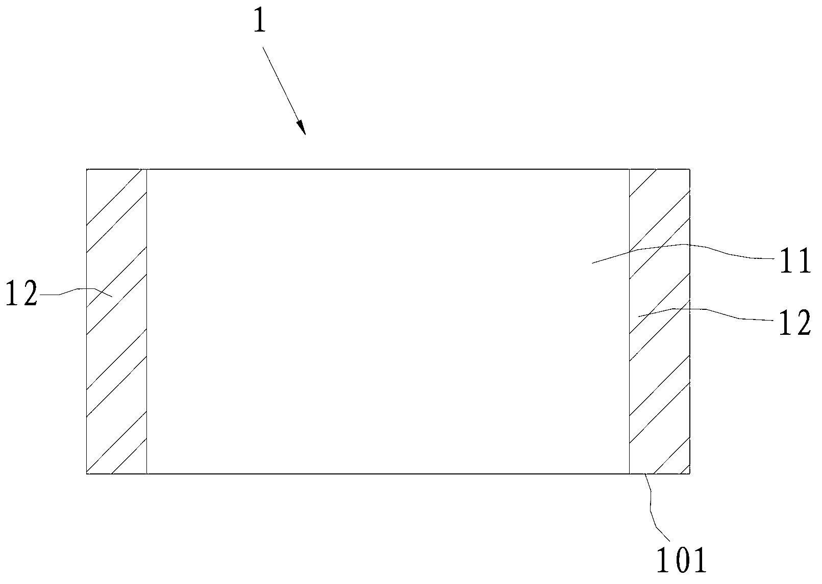
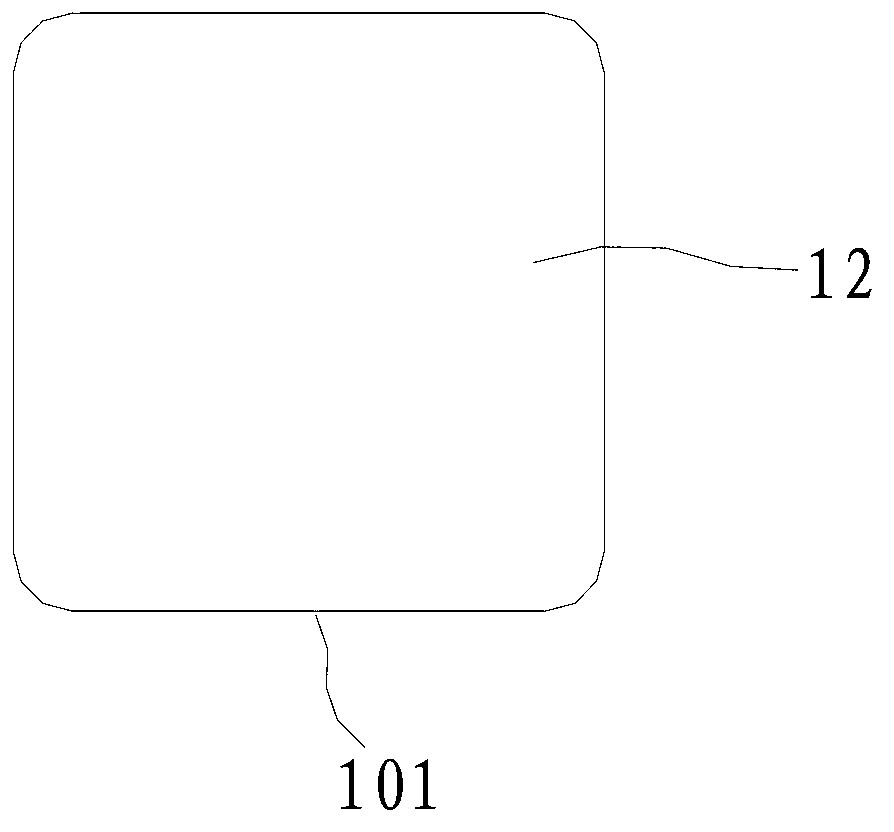
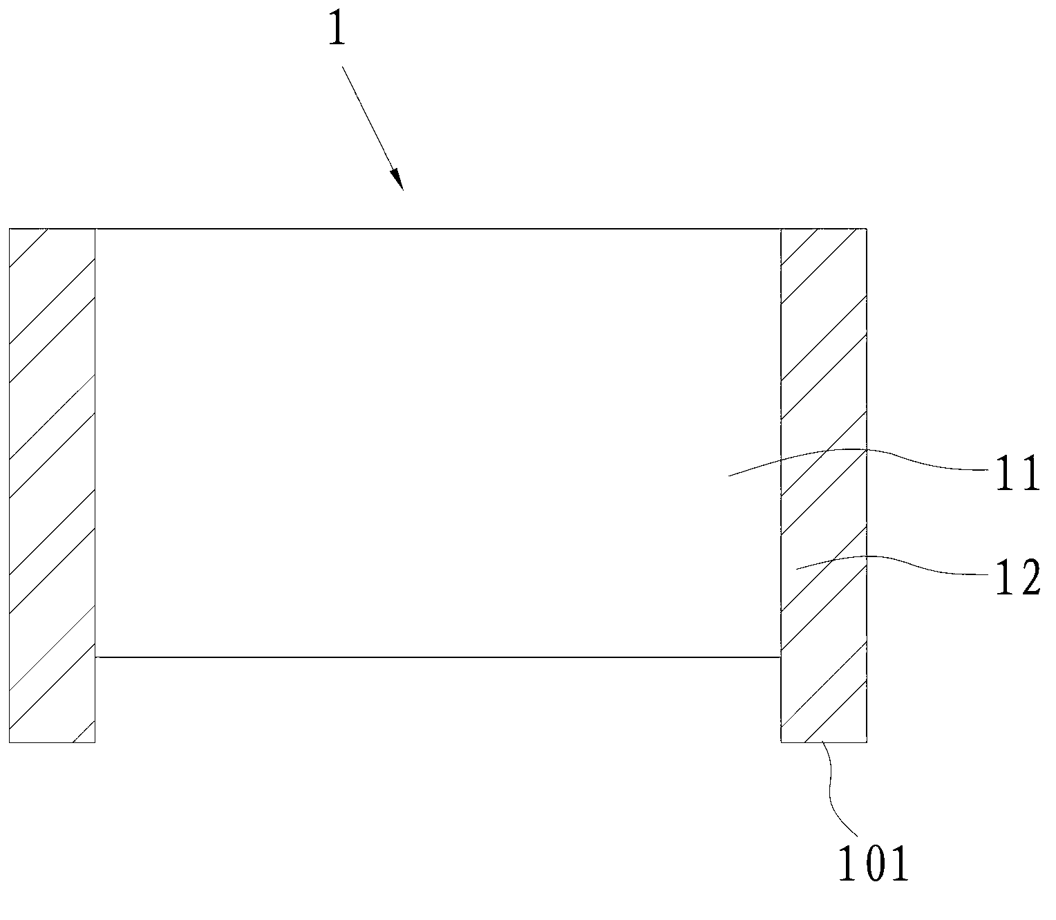
[0030] Such as figure 1 with figure 2 As shown, an electronic device 1 packaged with solder end rings provided by the embodiment of the present invention includes a body 11 and a solder end ring 12 , and the body 11 can be made of insulating materials such as ceramics and plastics. The welding end ring 12 is sleeved on the outer peripheral wall of the body 11 , and the welding end ring 12 may be annular. And the welding end ring 12 has a plane welding end 101 , and the plane welding end 101 is flush with the outer peripheral wall of the body 11 , that is, the end surface of the plane welding end 101 is flush with the lowest point of the outer peripheral wall of the body 11 . The outer peripheral wall of the body 11 can be cylindrical, and it is arranged transversely, and the end surface of the plane welding end 101 is tangent to the cylindrical body 11 . Cracks are not easy to occur at the solder joints and the application concentration is reduced. Even if cracks occur, the...

Embodiment 2

[0042] Such as Figure 7 with Figure 8 As shown, on the basis of the electronic device 1 packaged with the solder end ring 12 provided in Embodiment 1, the solder end ring 12 of the electronic device 1 in this embodiment also includes a middle solder end ring packaged in the middle section of the body 11 12. There can be two middle welding end rings 12 or other appropriate numbers, and the distance between the middle welding end rings 12 and the two end welding end rings 12 is set. The middle solder end ring 12 and the end solder ring 12 can be packaged in the body 11 through MELF. By adding the solder end ring 12 in the middle, compared with the electronic device 1 having only two solder end rings 12, the stress concentration of the solder end rings 12 at both ends can be effectively alleviated, and the stress can be distributed to each solder end ring 12, It is conducive to improving reliability; setting the contact mode between the solder end ring 12 and the pad to be s...


PUM


Abstract

The invention is suitable for the technical field of electronic devices and discloses an electronic device encapsulated with a welding end ring and electronic equipment provided with the electronic device. The electronic device comprises a body and the welding end ring, wherein the welding end ring is sleeved on the outer periphery wall of the body and provided with a plane welding end, and the plane welding end is flush with or extrudes out of the outer periphery wall. The electronic equipment comprises a circuit board and the electronic device encapsulated with the welding end ring, wherein a welding pad is arranged on the circuit board, and the plane welding end of the electronic device is welded on the welding pad. According to the electronic device encapsulated with the welding end ring and the electronic equipment provided with the electronic device, as the plane welding end which is flush with or extrudes out of the body is arranged, when the plane welding end is welded on the circuit board, cracks are not easy to generate at a welding spot, stress concentration is reduced, the expandable path of the cracks also becomes larger, so that the electronic device and the electronic equipment do not easily lose efficacy and are high in reliability.

Description

technical field [0001] The invention belongs to the technical field of electronic devices, and in particular relates to an electronic device packaged with a solder end ring and electronic equipment with the electronic device. Background technique [0002] Current electronic devices, such as MELF packaged devices, generally have a cylindrical soldering end, which is flush with the body, and the soldering end is in line contact with a pad of a PCB (Printed Circuit Board, printed circuit board), and the contact area is small. When this type of device in the prior art is soldered on the PCB, the height of the solder paste climbing along the soldering end is small, resulting in a small amount of tin at the soldering end. Since the body is ceramic, it does not match the CTE (Coefficient of Thermal Expansion, coefficient of thermal expansion) of the PCB, and the small amount of tin at the soldering end does not play a good role in reducing the mismatch of CTE, so in long-term opera...

Claims


Application Information

Patent Timeline
Patent Type & Authority Applications(China)
IPC IPC(8): H01L23/488
Inventor 杨巍华
Owner HUAWEI TECH CO LTD
Why Eureka
Try Eureka