Fast recovery diode and method for making same
A technology for recovering diodes and diodes, which is applied in semiconductor/solid-state device manufacturing, electrical components, circuits, etc., and can solve problems such as high reverse recovery voltage, hard reverse recovery, and adverse effects of circuits
- Summary
- Abstract
- Description
- Claims
- Application Information
AI Technical Summary
Problems solved by technology
Method used
Image
Examples
Embodiment Construction
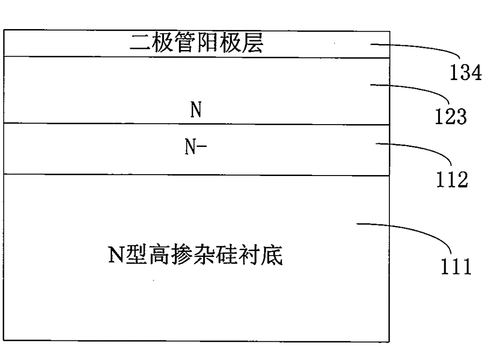
[0016] Please refer to figure 2 A preferred embodiment of the fast recovery diode of the present invention includes an N-type highly doped silicon substrate 111, a first N-type doped semiconductor layer 112, a second N-type doped semiconductor layer 123, and a diode anode layer 134 , the first N-type doped semiconductor layer 112 is located between the second N-type doped semiconductor layer 123 and the N-type highly doped silicon substrate 111 . Wherein the width of the first N-type doped semiconductor layer 112 is 5 μm to 50 μm, and the doping concentration is 5e12 / cm 3 -5e14 / cm 3 . The doping concentration N of the second N-type doped semiconductor layer 123 D and the width d of the second N-type doped semiconductor layer 123 satisfy the formula (1):
[0017] where ε in formula (1) r is the dielectric constant of silicon, ε 0 is the dielectric constant of vacuum, e refers to the electric charge of a single electron, V R is the reverse bias voltage for normal opera...
PUM
 Abstract
Description
Claims
Application Information


