
Optical fiber and optical electronic device vertical coupling method

An optoelectronic device, vertical coupling technology, applied in the coupling of optical waveguides and other directions, can solve the problems of difficult alignment, limited range of applicable devices, complex processes, etc., to facilitate large-scale production, improve accuracy, and realize arrayed coupling output Effect

Inactive Publication Date: 2013-10-09
INST OF SEMICONDUCTORS - CHINESE ACAD OF SCI
View PDF4 Cites 6 Cited by
  • Summary
  • Abstract
  • Description
  • Claims
  • Application Information

AI Technical Summary

Problems solved by technology

Traditional fiber coupling technologies include V-shaped grooves, optical waveguides, and making coupling fixtures, etc., but there are various limitations such as complex processes, difficult alignment, and limited range of applicable devices.
In particular, for the coupling output of quantum dot single photon source devices and optical fibers, since the size of self-organized quantum dots is only tens of nanometers, and the device size is on the order of microns, in order to isolate the single photon output of a single device from the pair of devices and optical fibers The quasi-precision puts forward new requirements, and the traditional coupling method is difficult to play a role

Method used


Image

  • Optical fiber and optical electronic device vertical coupling method

Examples


Embodiment Construction

[0019] In order to make the object, technical solution and advantages of the present invention clearer, the present invention will be described in further detail below in conjunction with specific embodiments and with reference to the accompanying drawings.

[0020] It should be noted that, in the drawings or descriptions of the specification, similar or identical parts all use the same figure numbers. Implementations not shown or described in the accompanying drawings are forms known to those of ordinary skill in the art. Additionally, while illustrations of parameters including particular values ​​may be provided herein, it should be understood that the parameters need not be exactly equal to the corresponding values, but rather may approximate the corresponding values ​​within acceptable error margins or design constraints. In addition, the directional terms mentioned in the following embodiments, such as "upper", "lower", "front", "rear", "left", "right", etc., are only re...


PUM


Abstract

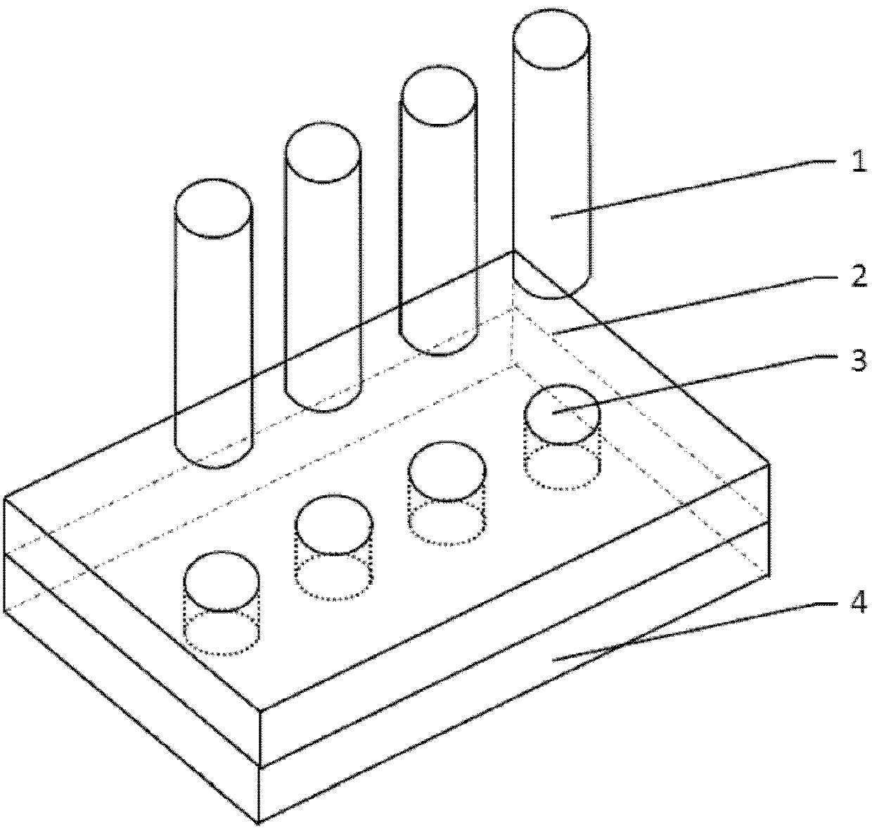
The invention discloses an optical fiber and optical electronic device vertical coupling method. The method comprises the steps that the surface of an optical electronic device is pre-coated by a layer of photoresist; an aligning hole array is formed in the surface of the optical electronic device through the photolithography; coating layers on the end portions of optical fibers are stripped to expose optical fiber inner cores; under the assistance of a microscope and a displacement platform, the optical fiber inner cores exposed out of the end portions of the optical fibers are inserted into aligning holes and fixed through colloid. The optical fiber and optical electronic device vertical coupling method is particularly applicable to optical fiber coupling output of optical electronic devices like single-photo sources which are small in light area and in need of spatial isolation, and has the advantages of being high in spatial resolution ratio and simple and reliable in technology.

Description

technical field [0001] The invention belongs to the technical field of semiconductor materials and devices, and relates to a method for vertically coupling optical fibers and optoelectronic devices based on SU-8 alignment holes. Background technique [0002] An important prerequisite for the application of optoelectronic devices is the coupling output with optical fibers. Among them, vertical emitting devices have been widely promoted as light sources due to their advantages such as arraying, low driving current, easy industrial production, low divergence angle, and good far-field symmetry. Traditional fiber coupling technologies include V-shaped grooves, optical waveguides, and coupling fixtures, but there are various limitations such as complex processes, difficult alignment, and limited range of applicable devices. In particular, for the coupling output of quantum dot single photon source devices and optical fibers, since the size of self-organized quantum dots is only te...

Claims


Application Information

Patent Timeline
Patent Type & Authority Applications(China)
IPC IPC(8): G02B6/42
Inventor 査国伟牛智川倪海桥李密锋喻颖王莉娟徐建星尚向军贺振宏
Owner INST OF SEMICONDUCTORS - CHINESE ACAD OF SCI
Learn More