Split-gate type flash memory structure and manufacturing method thereof

A split-gate flash memory and manufacturing method technology, which is applied in semiconductor/solid-state device manufacturing, electrical components, electrical solid-state devices, etc., can solve the problems of leakage current and other problems

Active Publication Date: 2013-10-09
SHANGHAI HUAHONG GRACE SEMICON MFG CORP
View PDF3 Cites 8 Cited by
  • Summary
  • Abstract
  • Description
  • Claims
  • Application Information

AI Technical Summary

Problems solved by technology

[0007] Moreover, it must be isolated between the polysilicon word line 1 and the control gate layer 5, that is, when the polysilicon word line 1 applies a high voltage to perform an erasing operation on the floating gate layer 3, the polysilicon word line 1 and the control gate layer 5 There can be no leakage current. In this case, an offset spacer must be introduced between the polysilicon word line 1 and the control gate layer 5, causing the control gate layer 5 to be shorter than the floating gate layer 3, such as figure 1 shown

Method used


Image

  • Split-gate type flash memory structure and manufacturing method thereof
  • Split-gate type flash memory structure and manufacturing method thereof
  • Split-gate type flash memory structure and manufacturing method thereof

Examples


Embodiment Construction

[0022] In order to make the content of the present invention clearer and easier to understand, the content of the present invention will be described in detail below in conjunction with specific embodiments and accompanying drawings.

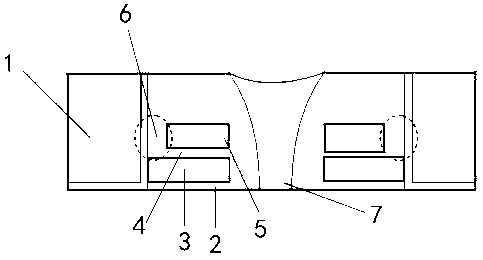
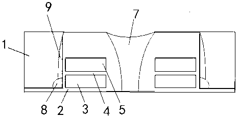
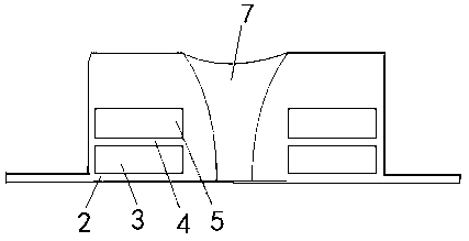
[0023] figure 2 A split-gate flash memory structure according to a preferred embodiment of the present invention is schematically shown.

[0024] Specifically, as figure 2 As shown, the split-gate flash memory structure according to the preferred embodiment of the present invention includes: two split-gate cells arranged side by side.

[0025] Each of the two sub-gate units arranged side by side includes a gate oxide layer 2 , a floating gate layer 3 , a control gate oxide layer 4 and a control gate layer 5 stacked in sequence.

[0026] Also, each of the two sub-gate units arranged side by side is entirely covered with oxide to form oxide sidewalls.

[0027] In the direction where two sub-gate units are arranged side by side, the size of th...


PUM


Abstract

The invention discloses a split-gate type flash memory structure and a manufacturing method of the split-gate type flash memory structure. The split-gate type flash memory structure comprises two split-gate units which are arranged in an abreast mode. Each split-gate unit comprises a gate electrode oxide layer, a floating gate layer, a control gate electrode oxide layer and a control gate electrode layer, wherein each gate electrode oxide layer, each floating gate layer, each control gate electrode oxide layer and each control gate electrode layer are arranged in a stacked mode in sequence. Each split-gate unit is integrally covered with oxide, and an oxide side wall is formed. The size of each floating gate layer is the same as the size of each control gate layer in the direction of abreast arrangement of the two split-gate units. A selection wire polycrystalline silicon area is arranged between the two split-gate units. A polycrystalline silicon connecting area and an oxide isolating area are formed on the oxide side wall on the outer side of each split-gate unit in a stacked mode, and the outer side of each split-gate unit is the other side, opposite to each selection wire polycrystalline silicon area, of each split-gate unit. Each polycrystalline silicon connecting area is flush with the upper surface of each floating gate layer. A polycrystalline silicon word line is formed on the outer side of each polycrystalline silicon connecting area and each oxide isolating area, wherein each polycrystalline silicon connecting area and each oxide isolating area are arranged in the stacked mode.

Description

technical field [0001] The invention relates to the field of semiconductor manufacturing, and more specifically, the invention relates to a split-gate flash memory structure and a manufacturing method thereof. Background technique [0002] Flash memory has become a research hotspot in non-volatile memory due to its convenience, high storage density, and good reliability. Since the first flash memory product came out in the 1980s, with the development of technology and the storage needs of various electronic products, flash memory has been widely used in mobile and communication devices such as mobile phones, notebooks, handheld computers and U disks. . [0003] figure 1 A split-gate structure of a flash memory according to the prior art is schematically shown. [0004] Such as figure 1 As shown, the split-gate structure of the flash memory according to the prior art includes two split-gate units. Each of the two sub-gate units includes a gate oxide layer 2 , a floating ...

Claims


Application Information

Patent Timeline
Patent Type & Authority Applications(China)
IPC IPC(8): H01L27/115H01L29/423H01L21/8247H01L21/28
Inventor 张雄方亮
Owner SHANGHAI HUAHONG GRACE SEMICON MFG CORP
Why Eureka
Try Eureka