Clamping circuit

A clamping circuit and voltage divider circuit technology, applied in the direction of circuits, electrical components, electric solid devices, etc., can solve the problems of increasing PCB area, being susceptible to interference, increasing costs and application circuit complexity, saving costs, improving Anti-interference performance, the effect of improving product competitiveness

Active Publication Date: 2013-10-09
SINO WEALTH ELECTRONICS
View PDF3 Cites 2 Cited by
  • Summary
  • Abstract
  • Description
  • Claims
  • Application Information

AI Technical Summary

Problems solved by technology

[0009] a. For the low-voltage MCU chip of CMOS process, it cannot directly withstand the mains AC 220V / 110V voltage and other forms of high voltage. figure 1 , 2 The diode D1 and transistor J1 are integrated in the chip, so it is necessary to integrate external components on the printed circuit board (PCB) to realize the AC zero-crossing detection function during application, which increases the cost of the user's application and the complexity of the application circuit degrees while increasing the area of ​​the PCB
[0010] b. Due to the use of external components and applications in high-voltage circuits, they are susceptible to interference

Method used


Image

  • Clamping circuit
  • Clamping circuit
  • Clamping circuit

Examples


Embodiment Construction

[0053] The present invention will be further explained below in conjunction with specific embodiments and drawings. In the following description, more details are set forth in order to fully understand the present invention. However, the present invention can obviously be implemented in many other ways different from the description herein. Those skilled in the art can make similar promotion and deduction according to actual application conditions without violating the connotation of the present invention. Therefore, the content of this specific embodiment should not limit the protection scope of the present invention.

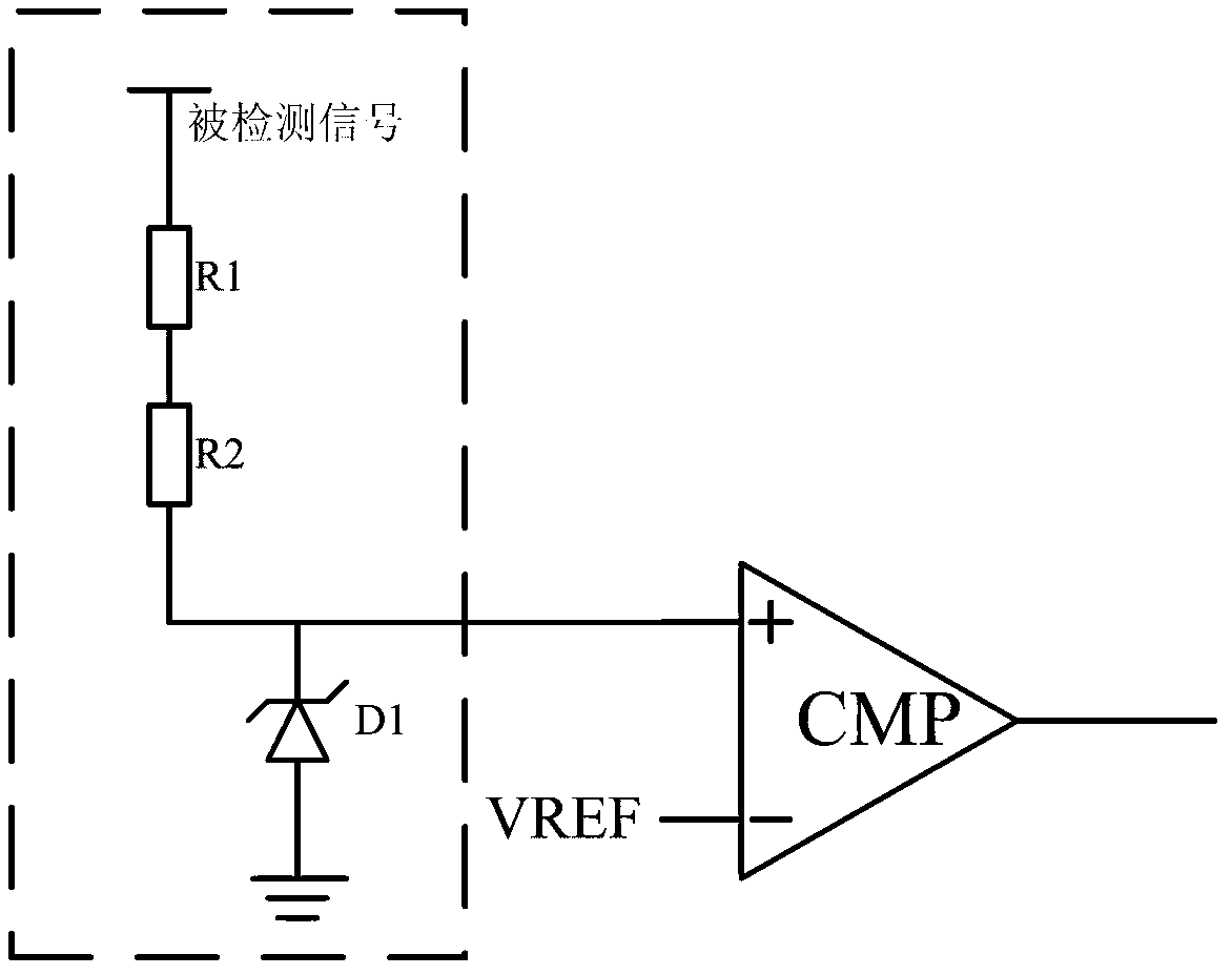
[0054] The present invention can completely integrate the external high-voltage zero-crossing comparison function inside the low-voltage MCU chip for realization, and the circuit principle is as follows:

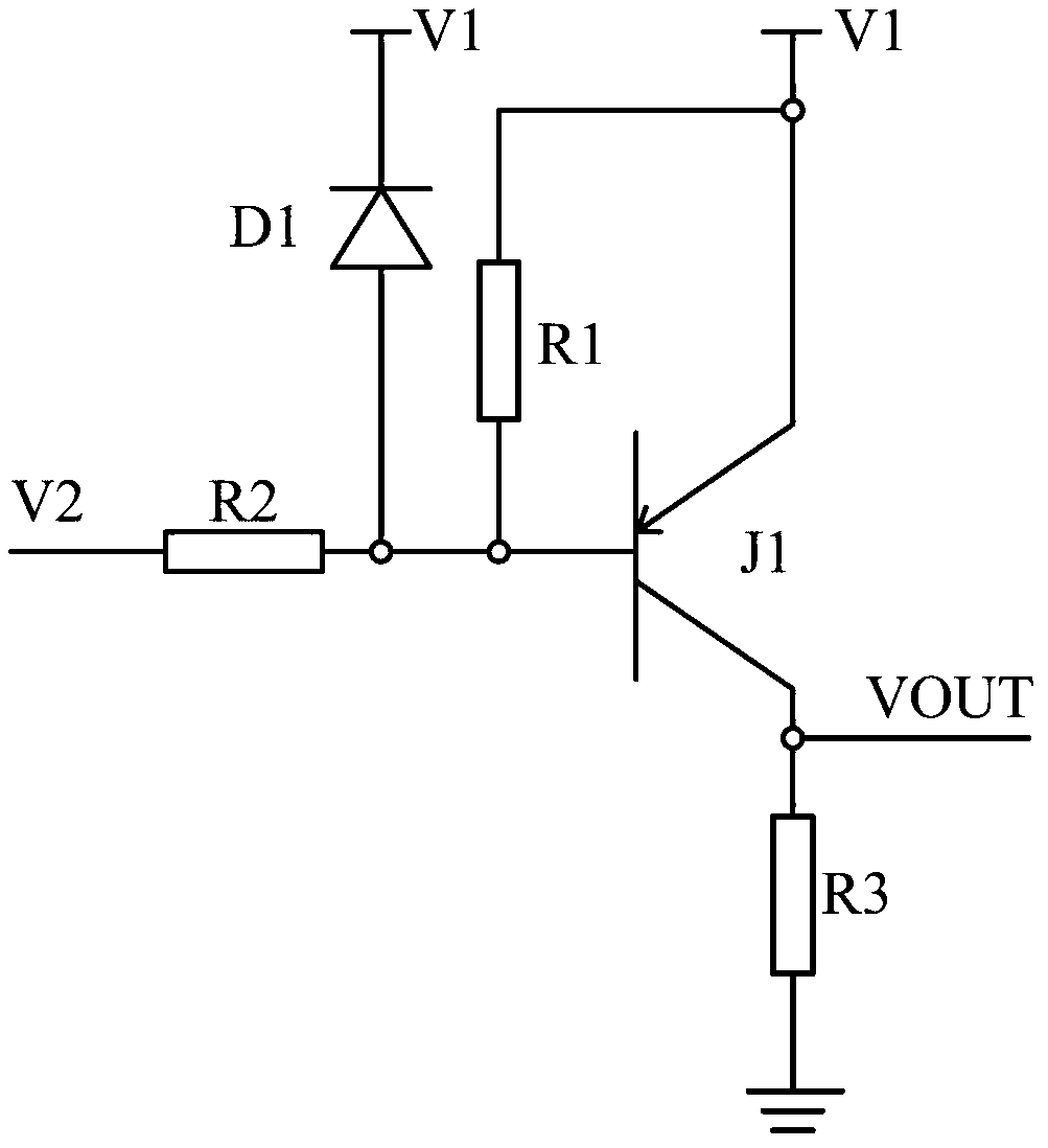
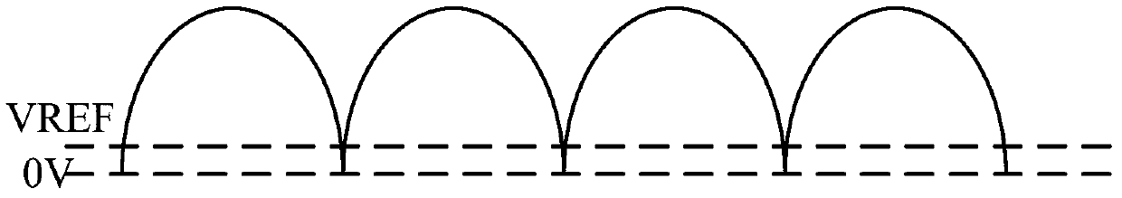
[0055] Figure 5 Is a schematic structural diagram of a clamping circuit according to an embodiment of the present invention; Image 6 It is a schematic diagram o...


PUM


Abstract

The invention provides a clamping circuit which is integrated inside a low-voltage MCU chip. The clamping circuit comprises a low-voltage NMOS pipe and a low-voltage PMOS pipe. A source electrode of the low-voltage NMOS pipe is connected with a low-voltage power source in the chip, and a substrate of the low-voltage NMOS pipe is connected with ground. A source electrode of the low-voltage PMOS pipe is connected with the ground, a substrate of the low-voltage PMOS pipe is connected with the low-voltage power source, and a drain electrode of the low-voltage PMOS pipe is connected with a drain electrode of the low-voltage NMOS pipe. A voltage leading-out point is formed on the connecting point of the drain electrode of the low-voltage PMOS pipe and the drain electrode of the low-voltage NMOS pipe, and the voltage leading-out point is connected with a high-voltage alternating-current level outside the chip. According to the clamping circuit, high-voltage alternating current signals which are excessive in amplitude are clamped within the largest withstand-voltage range which the low-voltage MCU chip can bear, and therefore an over-zero comparison function is integrated in a CMOS low-voltage technology, external elements are reduced, and cost is lowered.

Description

Technical field [0001] The present invention relates to the technical field of analog integrated circuit design. Specifically, the present invention relates to a clamp circuit applicable to zero-crossing detection. Background technique [0002] 1) Current product structure [0003] At present, the zero-crossing detection function applied to the SCR / relay control in the field of large and small home appliances is realized by integrating external components outside the low-voltage chip and on the PCB board. figure 1 with figure 2 . The meaning of zero-crossing detection is: the detection of the zero phase of the detected signal and a certain reference signal, that is, the voltage detection when the voltage is equal. [0004] 2) The principle of the current product [0005] Attached figure 1 The principle of the high-voltage zero-crossing detection application circuit shown in is: the detected signal is a high-voltage signal, which is stabilized below a certain voltage VCM through the ...

Claims


Application Information

Patent Timeline
Patent Type & Authority Applications(China)
IPC IPC(8): H02M5/293H01L27/00
Inventor 蒙蕾朱秉濬
Owner SINO WEALTH ELECTRONICS
Why Eureka
Try Eureka