NAND flash memory

A flash memory and storage unit technology, applied in the field of NAND flash memory, can solve the problems of high packaging and chip costs, complex operation, etc., and achieve the effect of improving data transmission speed, simple operation, and saving the number of I/O

Active Publication Date: 2013-10-23
GIGADEVICE SEMICON (BEIJING) INC
View PDF4 Cites 3 Cited by
  • Summary
  • Abstract
  • Description
  • Claims
  • Application Information

AI Technical Summary

Problems solved by technology

[0004] The traditional parallel interface Nand Flash has a large number of I / Os, the operation is more complicated, and the packaging and chip costs are also higher

Method used


Image

  • NAND flash memory
  • NAND flash memory
  • NAND flash memory

Examples


Embodiment 1

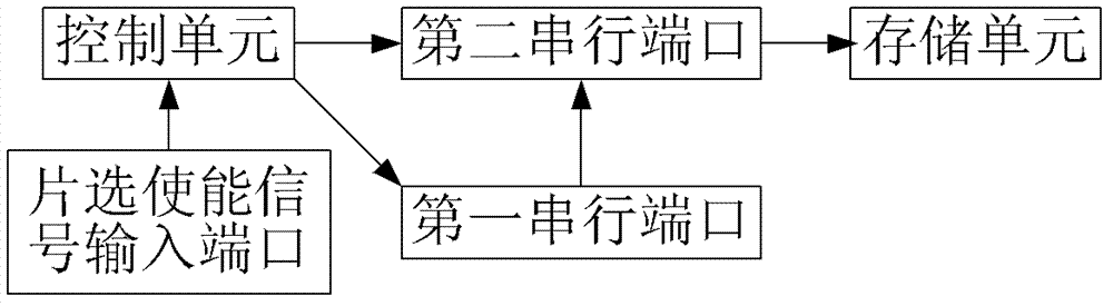
[0034] Embodiment one, a kind of NAND flash memory, such as figure 2 shown, including: storage unit;

[0035] a serial interface, including a first serial port and a second serial port;

[0036] The chip select enable signal input port is used to receive the chip select enable signal;

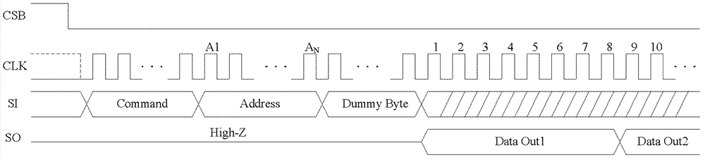
[0037] The control unit is used to indicate that the first serial port receives input data (including command signals, address signals, and sometimes empty bytes, etc.) when the chip select enable signal is low; after receiving the input data, Instructing the second serial port to output the data of the storage unit corresponding to the address.

[0038] In this embodiment, the NAND memory may further include a clock signal input port for receiving a clock signal for use by other devices in the NAND memory.

[0039] In this embodiment, the NAND memory may further include a buffer for saving the input data received by the first serial port for use when the second serial port outputs it.

[...

Embodiment 2

[0042] Embodiment 2, a NAND flash memory, has the same structure as Embodiment 1, and may also include the clock signal input port and buffer.

[0043] In this embodiment, the second serial port includes a first serial output port and a second serial output port, that is, a dual output (Dual Output) port is used.

[0044] In this embodiment, the control unit instructing the second serial port to output data corresponding to the address to the storage unit refers to:

[0045] The control unit instructs the first serial output port and the second serial output port to simultaneously output the data of the storage unit corresponding to the address.

[0046] Compared with the previous embodiment, this embodiment only needs half the clock time to transmit the same data, that is, the output data transmission speed is doubled.

[0047] Figure 4It is a timing diagram of this embodiment, and SO1 and SO2 are the data output to the storage unit by the first and second serial output po...

Embodiment 3

[0048] Embodiment 3, a NAND flash memory, has the same structure as Embodiment 1, and may also include the clock signal input port and buffer.

[0049] In this embodiment, the second serial port includes a first serial output port, a second serial output port, a third serial output port and a fourth serial output port, that is, a quad output (Quad Output) port.

[0050] In this embodiment, the control unit instructing the second serial port to output data corresponding to the address to the storage unit refers to:

[0051] The control unit instructs the first serial output port, the second serial output port, the third serial output port and the fourth serial output port to simultaneously output the data of the storage unit corresponding to the address.

[0052] In this embodiment, the output data is jointly transmitted by four ports, which can increase the output data transmission speed by four times.

[0053] Figure 5 It is a timing diagram of this embodiment, and SO1, S...


PUM


Abstract

The invention provides an NAND (Not And) flash memory which comprises a memory unit, a serial interface, a chip selection enable signal input port, and a control unit, wherein the serial interface comprises a first serial port and a second serial port; the chip selection enable signal input port is used for receiving a chip selection enable signal; and the control unit is used for indicating the first serial port to receive input data when the chip selection enable signal is at a low level, and indicating the second serial port to output the data of the memory unit with a corresponding address after the input data is received. The NAND flash memory can be provided with different interfaces; the application flexibility and the application scope of a chip are improved and extended; the IO (Input / Output) quantity is reduced; and the cost is lowered.

Description

technical field [0001] The invention relates to the storage field, in particular to a NAND flash memory. Background technique [0002] The timing diagram of the traditional parallel interface Nand Flash (flash memory) principle is as follows: figure 1 shown. [0003] CLE is the command latch enable (Commad latch enable) input port. When CLE is high, the command information is transmitted from I / O[7:0] to the on-chip command register on the rising edge of the WE# signal. When there is no need to load When loading (load) command information, the CLE signal should always be low; CE# is the chip select (Chip Enable) input port, which is active at low level; WE# is the write enable (Write Enable) input port, which is active at low level; ALE is the address latch enable (Address latch enable) input port. During the period when ALE is high, the address information is transferred from I / O[7:0] to the on-chip address register. When there is no need to load (load) the address When ...

Claims


Application Information

Patent Timeline
Patent Type & Authority Applications(China)
IPC IPC(8): G06F12/08G06F3/06G06F13/42
Inventor 苏志强丁冲张现聚
Owner GIGADEVICE SEMICON (BEIJING) INC
Why Eureka
Try Eureka