Non-volatile memory reading speed test circuit

A non-volatile, read-speed technology, applied in static memory, instruments, etc., to achieve accurate testing, high measurement accuracy, and easy implementation

Active Publication Date: 2013-10-23
SHANGHAI HUAHONG GRACE SEMICON MFG CORP
View PDF4 Cites 4 Cited by
  • Summary
  • Abstract
  • Description
  • Claims
  • Application Information

AI Technical Summary

Problems solved by technology

The test circuit introduces a test error due to the delay effect of the comparison circuit

Method used


Image

  • Non-volatile memory reading speed test circuit
  • Non-volatile memory reading speed test circuit

Examples


Embodiment Construction

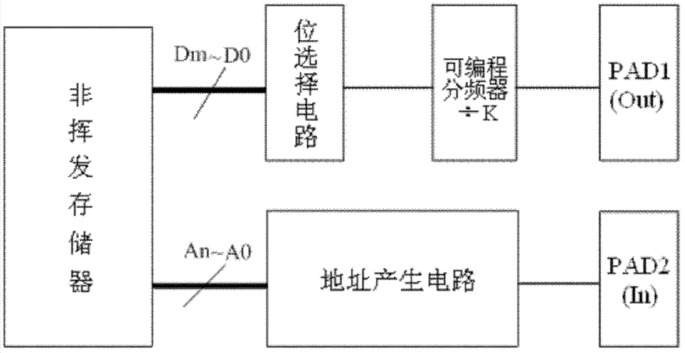
[0016] to combine figure 2 As shown, in an embodiment of the present invention, a FLASH whose output data bit width is 16 bits is taken as an example for description. The non-volatile memory reading speed test circuit includes: an address generation circuit, a bit selection circuit, and a programmable frequency divider. In the non-volatile memory, the data is pre-stored in a format in which every other address data is the same and adjacent address data is bit-inverse, and the data signals Dm-D0 are output according to the address jump of the address scanning signal. For example, address 0 stores 0xAAAA, address 1 stores 0x5555, and so on.

[0017] The address generating circuit generates an address scanning signal of the non-volatile memory under the drive of the external input clock (clock) input by the input pin PAD2, and continuously reads the non-volatile memory. For example, address scanning is realized by simply adding 1 to the address.

[0018] The data signals Dm-D...


PUM


Abstract

The invention discloses a test circuit for testing a non-volatile memory. The test circuit comprises an address generation circuit for generating an address scanning signal of the non-volatile memory under the driving of an external input clock and continuously reading the non-volatile memory, a bit selection circuit for selecting a certain bit data signal from data signals Dm-D0 output by the non-volatile memory as a reference, forming a square wave signal and testing the reading speed of the non-volatile memory, and a programmable frequency divider for performing frequency division on the square wave signals formed by the data signal selected by the bit selection circuit according to a set frequency division ratio and outputting a low-frequency signal. According to the test circuit, the time delay error of each control circuit in the test circuit is eliminated; the reading speed of the non-volatile memory can be accurately tested; the test precision is high; the speed differences of data bits can be compared by controlling the selection of data.

Description

technical field [0001] The invention relates to the field of semiconductor integrated circuit manufacturing, in particular to a non-volatile memory NVM (Non-Volatile Memory) reading speed test circuit. Background technique [0002] The current non-volatile memory read speed test circuit adopts figure 1 In the structure shown, the address generation circuit generates the access address An~A0 of the non-volatile memory under the drive of the external clock (input from the pin PAD), and the preset reference data is compared with the output data Dm~D0 of the non-volatile memory. The circuit is compared and the comparison result is obtained. The test circuit introduces a test error due to the delay effect of the comparison circuit. Contents of the invention [0003] The technical problem to be solved by the present invention is to provide a non-volatile memory reading speed testing circuit, which can accurately test the reading speed of the non-volatile memory without introdu...

Claims


Application Information

Patent Timeline
Patent Type & Authority Applications(China)
IPC IPC(8): G11C29/08
Inventor 赵锋
Owner SHANGHAI HUAHONG GRACE SEMICON MFG CORP
Why Eureka
Try Eureka