A kind of nand flash memory chip and its chip programming method during checkerboard inspection
A flash memory chip and programming method technology, applied in the storage field, can solve the problems of slow test speed, time-consuming, high test cost, etc., and achieve the effect of improving test speed, shortening test time and reducing test cost
- Summary
- Abstract
- Description
- Claims
- Application Information
AI Technical Summary
Problems solved by technology
Method used
Image

Examples
Embodiment 1
[0052] Embodiment one, a kind of NAND flash memory chip, comprises: main array, built-in sample generator;
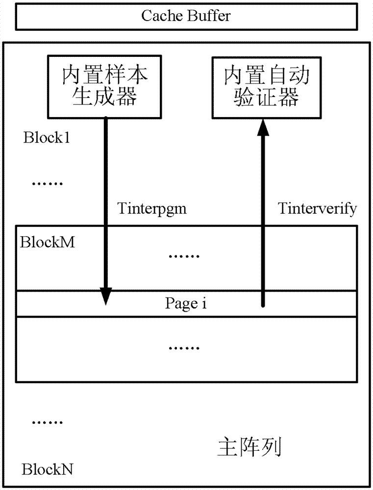
[0053] The control module is used to instruct the built-in sample generator to generate the sequence required for chip programming when the checkerboard check is to be performed; after the built-in sample generator generates the sequence, initiate a programming execution command to convert the sequence from The built-in sample generator is transferred to the main array for programming.
[0054] In this embodiment, the control module is further configured to initiate a WriteEnable (write enable) command before instructing the built-in sample generator to generate a sequence required for chip programming. If the command has been initiated before, the built-in sample generator can be directly instructed to generate the sequence required for chip programming.
[0055] In this embodiment, the control module can, but is not limited to, instruct the built-in sample ge...
Embodiment 2
[0068] Embodiment 2, a chip programming method during checkerboard inspection of a NAND flash memory chip, comprising:
[0069] When a checkerboard check is to be performed, the sequences required for chip programming are generated inside the chip;
[0070] After the sequence is generated, a programming execution command is initiated to transfer the generated sequence to the main array of the chip for programming.
[0071] In this embodiment, before generating the sequence required for chip programming, a WriteEnable (write enable) command is initiated first. If the command has been initiated before, the sequence required to program the chip can be directly generated.
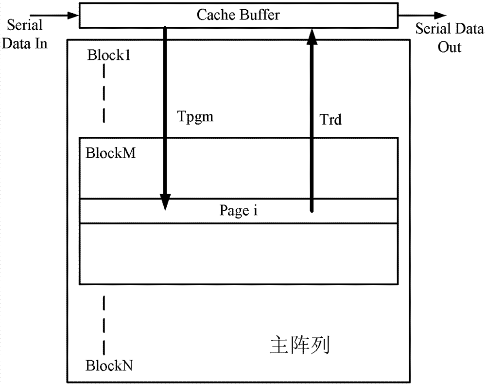
[0072] In this embodiment, the sequence required for chip programming may be generated, but not limited to, by executing a Programload (program loading) command. The Programload in this embodiment no longer needs to transfer DataBytes from the outside of the chip to the CacheBuffer one by one like t...
Embodiment 3
[0085] Embodiment three, a kind of NAND flash memory chip, comprises: main array, built-in automatic verifier;
[0086] The control module is used to read out the data in the main array page by page and transmit it to the built-in automatic verifier after the chip programming is completed;
[0087] The built-in automatic validator is used to validate the received data.
[0088] In this embodiment, the control module can, but is not limited to, execute the Pageread command to read the data in the main array page by page and send it to the built-in automatic verifier; different from the traditional method, after the Pageread command is initiated, it is no longer The data in the selected Page is first transmitted to the CacheBuffer, and then transmitted to the IO port by the CacheBuffer, but the data in the Page is transmitted to the "built-in automatic verifier (Internalautomaticverify)" to complete the CheckBoard verification directly, thus saving the data A large amou...
PUM
 Abstract
Description
Claims
Application Information
 - R&D
- Intellectual Property
- Life Sciences
- Materials
- Tech Scout
- Unparalleled Data Quality
- Higher Quality Content
- 60% Fewer Hallucinations
Browse by: Latest US Patents, China's latest patents, Technical Efficacy Thesaurus, Application Domain, Technology Topic, Popular Technical Reports.
© 2025 PatSnap. All rights reserved.Legal|Privacy policy|Modern Slavery Act Transparency Statement|Sitemap|About US| Contact US: help@patsnap.com