Formation method of fin field effect transistor

A technology of fin field effect transistors and fins, which is applied in the fields of electrical components, semiconductor/solid-state device manufacturing, circuits, etc., can solve device performance problems and other problems, and achieve the effects of good performance, inaccessibility, and small volume

Active Publication Date: 2015-09-02
SEMICON MFG INT (SHANGHAI) CORP
View PDF6 Cites 0 Cited by
  • Summary
  • Abstract
  • Description
  • Claims
  • Application Information

AI Technical Summary

Problems solved by technology

[0004] However, as the process node is further reduced, there are problems in the device performance of the prior art FinFET

Method used


Image

  • Formation method of fin field effect transistor
  • Formation method of fin field effect transistor
  • Formation method of fin field effect transistor

Examples


Embodiment Construction

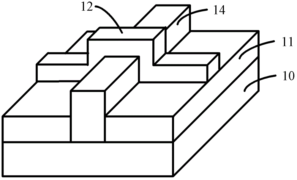
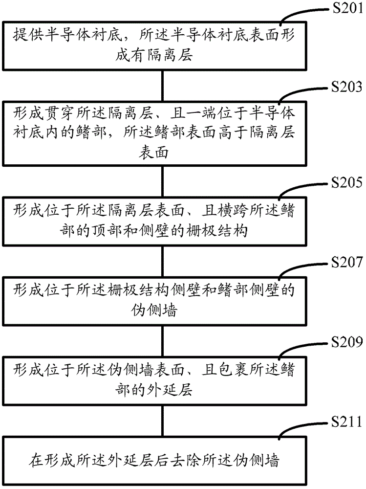
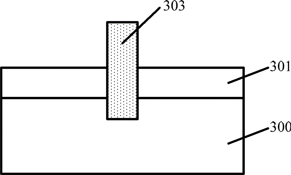
[0041] As mentioned in the background, in the prior art, as the process node is further reduced, the performance stability of the formed fin field effect transistor needs to be improved.

[0042] After research, the inventors found that with the further reduction of the process node, the distance between two adjacent fins is further reduced. After forming the gate structure, when the epitaxial layer wrapping the fins is formed, the The distance between the epitaxial layers of the two fins is difficult to control, and the formed epitaxial layers of the two adjacent fins are very easy to contact, which affects the subsequent process and seriously affects the performance of the FinFET.

[0043] Furthermore, the inventors found that before forming the epitaxial layer wrapping the fin, if dummy sidewalls are formed on the sidewalls of the fins, under the protection of the dummy sidewalls, the epitaxial layer is only formed on the undummy sidewalls. The surface of the fin covered by...


PUM


Abstract

Disclosed is a formation method for a fin field effect transistor (FET). The method includes: providing a semiconductor substrate; forming a separation layer at a surface of the semiconductor substrate; forming a fin part penetrating through the separation layer and one end of the fin part is in the semiconductor substrate and a surface of the fin part is higher than a surface of the separation layer; forming a gate structure which is arranged on the surface of the separation layer and stretches across a top and side walls of the fin part; and forming pseudo side walls arranged on side walls of the gate structure and side walls of the fin part; forming epitaxial layers which are arranged on surfaces of the pseudo side walls and wrap the fin part; and removing the pseudo side walls after the epitaxial layers are formed. The fin FET formed through the formation method provided by the embodiment of the invention is great in performance.

Description

technical field [0001] The invention relates to the technical field of semiconductor manufacturing, in particular to a method for forming a fin field effect transistor. Background technique [0002] With the continuous development of semiconductor process technology, process nodes are gradually reduced, and gate-last (gate-last) process has been widely used to obtain an ideal threshold voltage and improve device performance. However, when the feature size (CD, Critical Dimension) of the device is further reduced, even if the gate-last process is adopted, the structure of the conventional MOS field effect transistor can no longer meet the requirements for device performance, and the multi-gate device has been obtained as a substitute for the conventional device. Widespread concern. [0003] Fin field effect transistor (Fin FET) is a common multi-gate device. figure 1 A schematic diagram of a three-dimensional structure of a fin field effect transistor in the prior art is sh...

Claims


Application Information

Patent Timeline
Patent Type & Authority Patents(China)
IPC IPC(8): H01L21/336H01L29/78
Inventor 三重野文健
Owner SEMICON MFG INT (SHANGHAI) CORP
Why Eureka
Try Eureka