Infrared multi-wavelength absorber

A multi-wavelength absorber technology, which is applied in the field of infrared electromagnetic wave absorption and detection, can solve the problems of insensitivity to structural polarization, difficult control of absorption characteristics, and large thickness of resonant absorbers, so as to achieve simple structure, easy control of absorption characteristics, and improved The effect of sensitivity

Inactive Publication Date: 2013-10-23
NORTHWESTERN POLYTECHNICAL UNIV
View PDF10 Cites 13 Cited by
  • Summary
  • Abstract
  • Description
  • Claims
  • Application Information

AI Technical Summary

Problems solved by technology

[0007] In order to overcome the shortcomings of the traditional resonant absorber, such as large thickness, difficult control of absorption characteristics, and insensitivity to polarization of the existing metamaterial dual-wavelength absorber structure, the present invention proposes a resonant absorber that is easy to control thickness and absorption characteristics, and has polarization characteristics. Infrared Multi-Wavelength Absorber

Method used


Image

  • Infrared multi-wavelength absorber
  • Infrared multi-wavelength absorber
  • Infrared multi-wavelength absorber

Examples


Embodiment 1

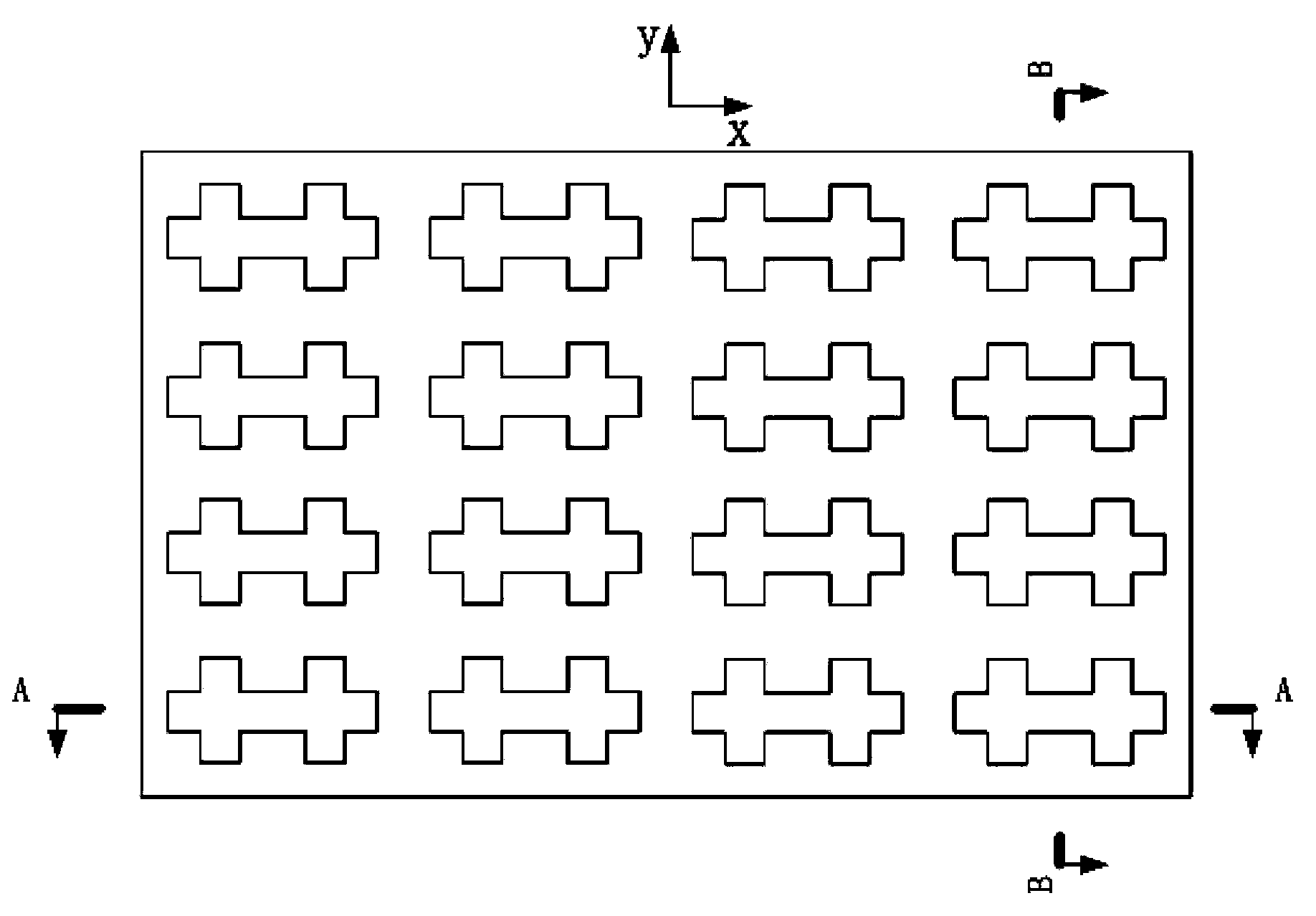
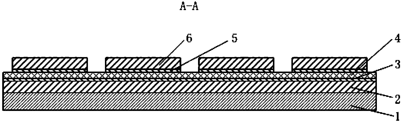
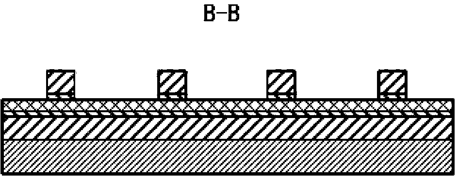
[0023] See attached figure 1 , with figure 2 , with image 3 , the infrared dual-wavelength absorber proposed by the present invention includes substrate I1, structural layer I2, adhesive layer I3, dielectric layer 4, adhesive layer II5 and structural layer II6 in sequence, the material of the substrate I1 is Si, the structural layer I2 and the structural layer The material of layer Ⅱ6 is Au, the material of adhesion layer Ⅰ3 and adhesion layer Ⅱ5 is Ti, and the material of dielectric layer 4 is Al 2 o 3 The length of the double cross structure in the x direction is 1.2 μm, the length in the y direction is 0.8 μm, the width of the double cross arms is 0.3 μm, the period in the x direction is 2 μm, and the period in the y direction is 1.2 μm; The thickness of the dielectric layer 4 is 0.05 μm, and the thickness of the adhesion layer I3 and the adhesion layer II5 is 5 nm. See attached Figure 4 , the infrared multi-wavelength absorber achieves absorptivity of 99.43%, 89.24...

Embodiment 2

[0025] See attached figure 1 , with figure 2 , with image 3 , the infrared dual-wavelength absorber proposed by the present invention includes substrate I1, structural layer I2, adhesive layer I3, dielectric layer 4, adhesive layer II5 and structural layer II6 in sequence, the material of the substrate I1 is Si, the structural layer I2 and the structural layer The material of layer Ⅱ6 is Au, the material of adhesion layer Ⅰ3 and adhesion layer Ⅱ5 is Ti, and the material of dielectric layer 4 is Al 2 o 3 The length of the double cross structure in the x direction is 1.4 μm, the length in the y direction is 0.8 μm, the width of the double cross arms is 0.3 μm, the period in the x direction is 2 μm, and the period in the y direction is 1.2 μm; The thickness of the dielectric layer 4 is 0.05 μm, and the thickness of the adhesion layer I3 and the adhesion layer II5 is 5 nm. See attached Figure 5 , the infrared multi-wavelength absorber achieves absorptivity of 99.83%, 88.19...

Embodiment 3

[0027] See attached figure 1 , with figure 2 , with image 3 , the infrared dual-wavelength absorber proposed by the present invention includes substrate I1, structural layer I2, adhesive layer I3, dielectric layer 4, adhesive layer II5 and structural layer II6 in sequence, the material of the substrate I1 is Si, the structural layer I2 and the structural layer The material of layer Ⅱ6 is Au, the material of adhesion layer Ⅰ3 and adhesion layer Ⅱ5 is Ti, and the material of dielectric layer 4 is Al 2 o 3 The length of the double cross structure in the x direction is 1.6 μm, the length in the y direction is 0.8 μm, the width of the double cross arms is 0.3 μm, the period in the x direction is 2 μm, and the period in the y direction is 1.2 μm; The thickness of the dielectric layer 4 is 0.05 μm, and the thickness of the adhesion layer I3 and the adhesion layer II5 is 5 nm. See attached Image 6 , the infrared multi-wavelength absorber achieves absorptivity of 99.34%, 85.34%...


PUM

PropertyMeasurementUnit
thicknessaaaaaaaaaa
thicknessaaaaaaaaaa
thicknessaaaaaaaaaa

Abstract

The invention discloses an infrared multi-wavelength absorber, which comprises a substrate I 1, a structural layer I 2, an adhesive layer I 3, a dielectric layer 4, an adhesive layer II 5 and a structural layer II 6 in sequence, wherein the structural layer II 6 consists of a double cross structure array; the double cross structures are formed by splicing two cross structures; the angles of arrays in both x and y directions are 90 degrees; and the cycles in both x and y directions are of wavelength scale. According to the infrared multi-wavelength absorber, multi-wavelength absorption of an infrared band is realized by using the structure arrays of a single size; the infrared multi-wavelength absorber has a simple structural form and small thickness and is easy in control of the absorption characteristic; and the infrared multi-wavelength absorber has polarization characteristic and has broad application prospect in the application aspect of biosensors. A large volume of experimental data proves that the infrared multi-wavelength absorber has superior performance.

Description

[0001] Field [0002] The invention relates to an infrared electromagnetic wave absorber, in particular to an infrared multi-wavelength absorber based on a double cross structure and having polarization characteristics, belonging to the technical field of infrared electromagnetic wave absorption and detection. Background technique [0003] Infrared absorbers are the basic building blocks for making devices such as photodetectors, microbolometers, solar photovoltaic thermal converters, and thermal imaging systems. Traditional infrared electromagnetic wave resonant absorbers are implemented using multilayer structures separated by quarter-wavelength dielectric layers. When applying this kind of resonance absorber, there are some difficult problems to solve. First, the thickness of the absorber is required to be at least a quarter wavelength, and if these absorbing layers are connected in series, their thickness must be increased significantly in order to broaden the performance...

Claims


Application Information

Patent Timeline
Patent Type & Authority Applications(China)
IPC IPC(8): H01Q17/00G02F1/01
Inventor 黎永前苏磊寿宸
Owner NORTHWESTERN POLYTECHNICAL UNIV
Why Eureka
Try Eureka