Surface checking method of printed circuit board

A printed circuit board, surface inspection technology, used in measuring devices, material analysis by optical means, instruments, etc., can solve the problems of distinguishing copper surface from substrate, inability to detect conditions, and inability to inspect quality.

Inactive Publication Date: 2013-10-30
ZHENJIANG HUAYANG INFORMATION TECH
View PDF7 Cites 8 Cited by
  • Summary
  • Abstract
  • Description
  • Claims
  • Application Information

AI Technical Summary

Problems solved by technology

[0005]1) When the surface of the printed circuit board is oxidized, the automatic optical inspection equipment cannot distinguish whether it is the oxidized part of the surface of the printed circuit board or the real defect on the surface of the printed circuit board;
[0006]2) There are many types of printed circuit board substrates, and the optical properties of different substrates are different. After replacing the substrate, it is necessary to re-adjust the parameters of the automatic optical inspection equipment , otherwise, the error rate of the detection result increases
[0007]3) After the surface of the printed circuit board is roughened, the reflective ability of the copper surface becomes poor, and the automatic optical

Method used


Image

  • Surface checking method of printed circuit board

Examples


Embodiment Construction

[0016]

[0017] A method for surface inspection of a printed circuit board provided by the technical solution will be further described in detail below in conjunction with an embodiment

[0018] A method for surface inspection of a printed circuit board provided in this embodiment includes the following steps:

[0019] The first step is to scan the surface of the printed circuit board with laser to obtain the three-dimensional structure of the surface of the circuit board;

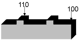
[0020] In this embodiment, the semi-finished printed circuit board (the inner layer circuit or the outer layer circuit has been produced) that needs to be inspected on the surface is placed on a flat table. A laser scanning system scans the surface of the circuit board in a non-contact manner. Laser systems can be designed using the principle of triangulation ranging. The image obtained by scanning is a three-dimensional image of the surface of the circuit board; the three-dimensional image mainly inclu...


PUM


Abstract

The invention relates to a surface checking method of a printed circuit board. The surface checking method comprises the following steps of: performing laser scanning on the surface of the printed circuit board to obtain a three-dimensional structure of the surface of the circuit board; converting the three-dimensional structure of the surface of the printed circuit board into a two-dimensional planar image; and contrasting the two-dimensional planar image with a design configuration of the surface of the printed circuit board so as to determine defect information of the surface of the circuit board. With the method, even if the surface of the printed circuit board is oxidized or roughed, various defects of the surface of the printed circuit board also can be detected; during the checking process, detection parameters do not need to be adjusted according to the type of a base material of the printed circuit board; meanwhile, information such as copper layer thickness also can be obtained, and more data is provided for understanding a manufacturing technology of the printed circuit board better.

Description

technical field [0001] The invention relates to the technical field of printed circuit board manufacturing, in particular to the quality inspection of printed circuit boards. Background technique [0002] With the fierce competition in the market, printed circuit board enterprises must ensure the quality of products, including long-term usability, electrical performance, etc., in order to occupy a place in the fiercely competitive market. Therefore, printed circuit board companies have strengthened the quality monitoring of each production link; at the same time, the graphics of printed circuit board circuits are becoming more and more refined, and the previous methods of visual inspection or manual optical inspection of printed circuit boards have been eliminated. It cannot adapt to the requirements of the market and technological development for printed circuit boards. Therefore, automatic optical inspection technology has been used on a large scale as a technical means o...

Claims


Application Information

Patent Timeline
IPC IPC(8): G01N21/956
Inventor 陈小芳
Owner ZHENJIANG HUAYANG INFORMATION TECH
Why Eureka
Try Eureka