Light emitting diode crystal grain and light emitting diode packaging structure using same

A technology of light-emitting diodes and grains, applied in semiconductor devices, electrical components, circuits, etc., can solve the problems of uneven light output and weak light intensity of light-emitting diode grains 100, and achieve the effect of increasing the light output range and uniform light output effect

Active Publication Date: 2013-10-30
ZHANJING TECH SHENZHEN +1
View PDF4 Cites 10 Cited by
  • Summary
  • Abstract
  • Description
  • Claims
  • Application Information

AI Technical Summary

Problems solved by technology

[0003] see figure 1 and figure 2 , in the prior art, the light emitting angle of the LED grain 100 is generally 90° to 120°, the light intensity in the center of the light emitting angle (the light emitting angle is about 0° to 30°) is strong, and the surrounding light intensity is weak, resulting in the entire Uneven light emission from LED grain 100

Method used


Image

  • Light emitting diode crystal grain and light emitting diode packaging structure using same
  • Light emitting diode crystal grain and light emitting diode packaging structure using same
  • Light emitting diode crystal grain and light emitting diode packaging structure using same

Examples


Embodiment Construction

[0024] The following will be combined with Figure 3-12 The present invention is described in further detail.

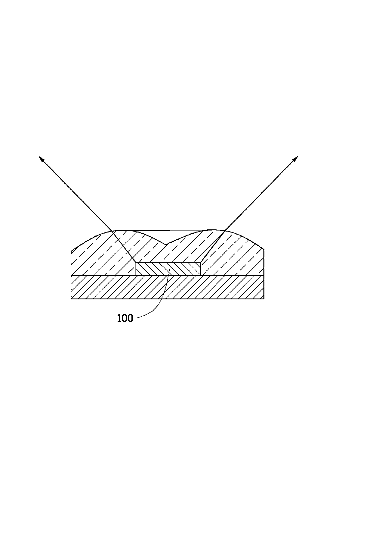
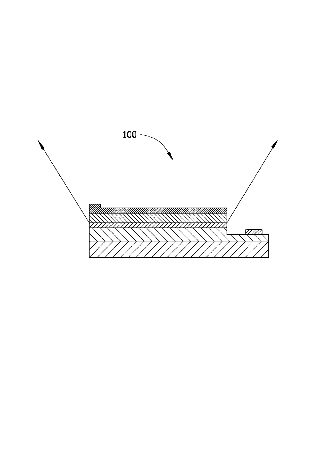
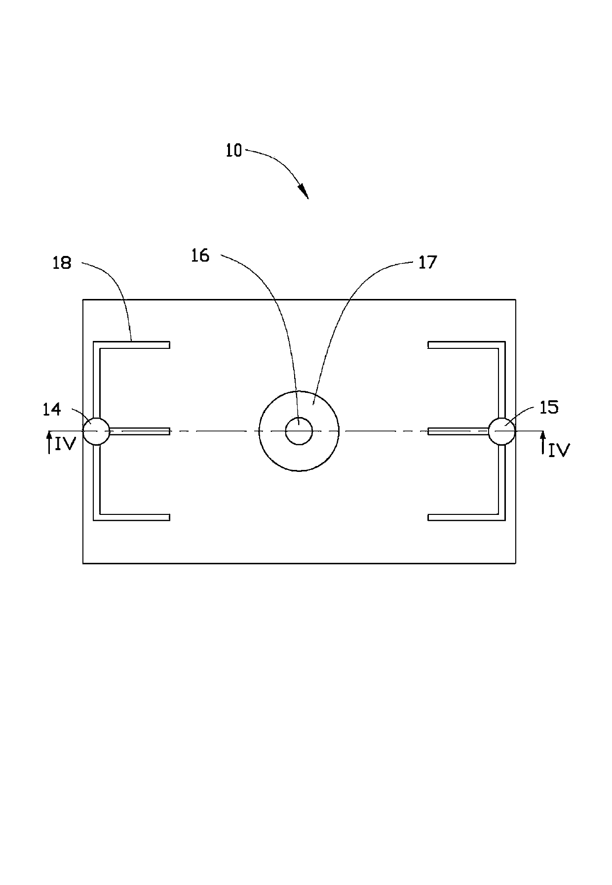
[0025] see Figure 4 The LED die 10 according to the first embodiment of the present invention includes a substrate 11 , an epitaxial layer 12 , a transparent conductive layer 13 , a first electrode 14 , a second electrode 15 and a common electrode 16 .

[0026] The material of the substrate 11 may be one of sapphire (Al2O3), silicon carbide (SiC), silicon (Si), gallium nitride (GaN) or zinc oxide (ZnO).

[0027] The epitaxial layer 12 includes a first semiconductor layer 121 , a second semiconductor layer 123 and an active layer 122 sandwiched between the first semiconductor layer 121 and the second semiconductor layer 123 . The first semiconductor layer 121 , the active layer 122 and the second semiconductor layer 123 are sequentially disposed on the substrate 11 . In this embodiment, the first semiconductor layer 121 and the second semiconductor layer 123 are s...


PUM

PropertyMeasurementUnit
light emitting angleaaaaaaaaaa

Abstract

An LED die comprises a substrate and an epitaxial layer formed thereon. The epitaxial layer comprises a first n-type semiconductor layer, an active layer and a p-type semiconductor layer grown on the substrate in sequence. The LED die defines a receiving recess formed in a center of a top face of the p-type semiconductor layer. The receiving recess extends through the p-type semiconductor layer, the active layer and into the n-type semiconductor layer along a top-to-bottom direction of the epitaxial layer. A pair of p-pads are located at two opposite sides of the p-type semiconductor layer, respectively. A first n-pad is received in the receiving recess and located on the n-type layer.

Description

technical field [0001] The invention relates to a semiconductor structure, in particular to a light emitting diode crystal grain and a light emitting diode packaging structure using the light emitting diode crystal grain. Background technique [0002] As a high-efficiency light source, light-emitting diodes have many characteristics such as environmental protection, power saving, and long life, and have been widely used in various fields. [0003] see figure 1 and figure 2 , in the prior art, the light emitting angle of the LED grain 100 is generally 90° to 120°, the light intensity in the center of the light emitting angle (the light emitting angle is about 0° to 30°) is strong, and the surrounding light intensity is weak, resulting in the entire The light emitted by the LED die 100 is not uniform. In order to improve the light uniformity of the light emitting diode grain 100, a lens is often formed directly above the light emitting diode grain 100. The light emitting d...

Claims


Application Information

Patent Timeline
Patent Type & Authority Applications(China)
IPC IPC(8): H01L33/02
CPCH01L33/54H01L33/58H01L33/62H01L33/20H01L33/38H01L2924/0002H01L2924/00
Inventor 沈佳辉洪梓健
Owner ZHANJING TECH SHENZHEN
Why Eureka
Try Eureka