Manufacturing method of combined printed circuit board, printed circuit board and manufacturing method thereof
A technology for printed circuit boards and manufacturing methods, which is applied in the direction of multilayer circuit manufacturing, printed circuit parts, and electrical connection formation of printed components, and can solve problems affecting PCB performance and low manufacturing precision of laminated circuit boards, and achieve Improve rigidity, not easily deformed, and ensure the effect of electrical connection
- Summary
- Abstract
- Description
- Claims
- Application Information
AI Technical Summary
Problems solved by technology
Method used
Image

Examples
Embodiment 1
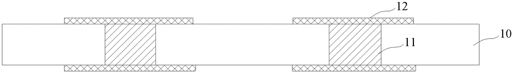
[0096] Embodiment 1. The PCB includes at least one of the above-mentioned combined printed circuit boards and a conductive layer located on at least one outer surface;
[0097] Taking a 4-layer PCB as an example, the 4-layer PCB includes metal foils on the two outer surfaces and a combined printed circuit board on the inner layer. The manufacturing process is as follows Figure 11 Shown include:
[0098] Step 1101, stacking process, stacking two metal foils 1201 and one combined printed circuit board 1202 in the order of metal foil→combined printed circuit board→metal foil, such as Figure 12A As shown, the two insulating substrates of the combined printed circuit board are respectively combined with two metal foils;
[0099] Specifically, the metal foil 1201 can be copper foil, or other metal materials, and its thickness is above 3 μm;
[0100] Step 1102, lamination treatment, wherein the temperature of the lamination treatment is higher than the glass transition temperatur...
Embodiment 2
[0110] Embodiment 2, the PCB includes at least one combined printed circuit board, a conductive layer located on at least one outer surface, and at least one metal-clad plate filled with conductive paste;
[0111] Taking an 8-layer PCB as an example, the 8-layer PCB includes: metal foils on the two outer surfaces, two combined printed circuit boards on the inner layer, and a conductive paste filled between the two combined printed circuit boards. The metal clad plate, its manufacturing process such as Figure 15 Shown include:
[0112] Step 1501, stacking process, two metal foils 1601, two combined printed circuit boards 1602a and 1602b and a metal-clad plate 1603 filled with conductive paste are processed according to the order of metal foil→combined printed circuit board→filled with conductive paste The sequence of metal clad plate→combined printed circuit board→metal foil is combined and stacked, such as Figure 16A shown;
[0113] Step 1502, lamination treatment, wherei...
Embodiment 3
[0118] Embodiment 3, the PCB includes at least one combined printed circuit board and a metal-clad plate located on at least one outer surface;
[0119] Taking a 6-layer PCB as an example, the 6-layer PCB includes: metal-clad plates on the two outer surfaces, and a combined printed circuit board on the inner layer. The manufacturing process is as follows: Figure 17 Shown include:
[0120] Step 1701, stacking boards, combining two metal-clad boards 1801 and a combined printed circuit board 1802 in the order of metal-clad boards→combined printed circuit boards→metal-clad boards, such as Figure 18A shown;
[0121] Wherein the metal-clad board 1801 includes an insulating layer and metal foils located on the two outer surfaces of the metal-clad board 1801. It should be noted that the metal foil in the metal-clad board 1801 that is in contact with the combined printed circuit board is processed before lamination. Pattern transfer is necessary to form a conductive layer with cond...
PUM
 Abstract
Description
Claims
Application Information
 - R&D
- Intellectual Property
- Life Sciences
- Materials
- Tech Scout
- Unparalleled Data Quality
- Higher Quality Content
- 60% Fewer Hallucinations
Browse by: Latest US Patents, China's latest patents, Technical Efficacy Thesaurus, Application Domain, Technology Topic, Popular Technical Reports.
© 2025 PatSnap. All rights reserved.Legal|Privacy policy|Modern Slavery Act Transparency Statement|Sitemap|About US| Contact US: help@patsnap.com