Detection system and method of semiconductor two-dimensional electron gas circular polarization spin photocurrent

A two-dimensional electron gas, circularly polarized spin technology, applied in the direction of a single semiconductor device testing, measuring current/voltage, measuring devices, etc., can solve the problems of reduced operability and reliability, and cannot improve defects, and achieve enhanced reliability. performance and superiority, suppression of amplification, effect of increased sensitivity

Inactive Publication Date: 2013-11-06
NANTONG UNIVERSITY
View PDF2 Cites 10 Cited by
  • Summary
  • Abstract
  • Description
  • Claims
  • Application Information

AI Technical Summary

Problems solved by technology

However, the above-mentioned improvement methods have greatly reduced the operability and reliability of the experimental system.
Moreover, the proposal of these methods can

Method used


Image

  • Detection system and method of semiconductor two-dimensional electron gas circular polarization spin photocurrent
  • Detection system and method of semiconductor two-dimensional electron gas circular polarization spin photocurrent

Examples


Embodiment 1

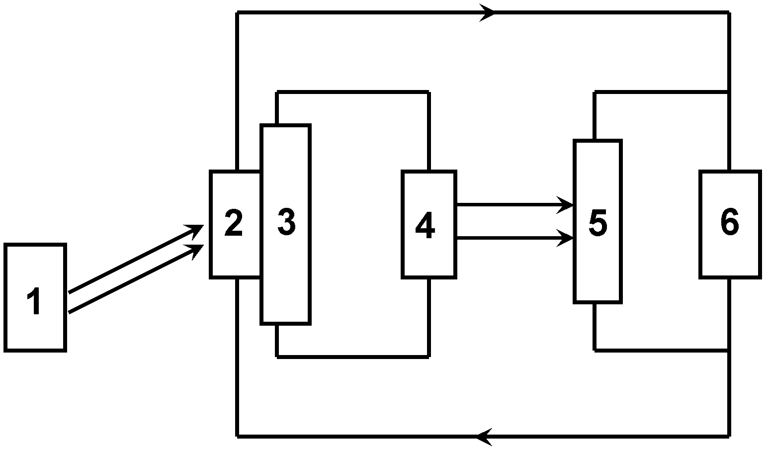
[0028] See figure 1 , the detection system of the semiconductor two-dimensional electron gas circularly polarized spin photocurrent in this embodiment includes a monochromatic circularly polarized light source 1, a semiconductor two-dimensional electron gas sample 2, a piezoelectric ceramic sheet 3, a high-voltage AC signal source 4, and a lock-in amplifier 5 and resistor 6.

[0029] A monochromatic circularly polarized light source 1 obliquely illuminates a semiconductor two-dimensional electron gas sample 2 . The piezoelectric ceramic sheet 3 exerts periodically changing stress on the semiconductor two-dimensional electron gas sample 2 . The high-voltage AC signal source 4 provides driving voltage to the piezoelectric ceramic sheet 3 . The resistor 6 is connected in series with the semiconductor two-dimensional electron gas sample 2 to form a loop. The lock-in amplifier 5 detects the current flowing through the resistor 6 . In the figure, the arrow between the monochroma...


PUM

PropertyMeasurementUnit
Thicknessaaaaaaaaaa
Thicknessaaaaaaaaaa
Thicknessaaaaaaaaaa

Abstract

The invention discloses a detection system and method of a semiconductor two-dimensional electron gas circular polarization spin photocurrent. The detection system comprises a monochromatic circular polarization light source, a semiconductor two-dimensional electron gas sample, a piezoelectric ceramic slice, a high-voltage alternating-current signal source, a lock-in amplifier and a resistor, wherein the monochromatic circular polarization light source illuminates the semiconductor two-dimensional electron gas sample in an inclining mode, the piezoelectric ceramic slice applies stress which changes periodically on the semiconductor two-dimensional electron gas sample, the high-voltage alternating-current signal source provides drive voltage for the piezoelectric ceramic slice, the resistor is connected with the semiconductor two-dimensional electron gas sample in series so that a loop can be formed, and the lock-in amplifier detects the current flowing through the resistor. The detecting system of the semiconductor two-dimensional electron gas circular polarization spin photocurrent is high in detection sensitivity, and improves the reliability and the superiority of the CPGE technology.

Description

technical field [0001] The invention relates to a detection system and a detection method for a semiconductor two-dimensional electron gas circularly polarized spin photocurrent. Background technique [0002] Semiconductor spintronics is an emerging discipline for the development of new electronic devices such as spin field effect transistors. This new type of spintronic devices will have obvious advantages in terms of power consumption, integration density, and data processing speed. The semiconductor two-dimensional electron gas system is the core structure of the above-mentioned new spintronic devices and physical research. Efficient injection of spin photocurrent into this two-dimensional electron gas system and high-sensitivity detection are prerequisites for the development of spintronics and spintronic devices. [0003] The photocurrent measurement technology based on the circular polarization photoelectric effect, referred to as the circular polarization spin photo...

Claims


Application Information

Patent Timeline
IPC IPC(8): G01R19/00G01R31/26
Inventor 余晨辉罗向东刘培生徐炜炜
Owner NANTONG UNIVERSITY
Why Eureka
Try Eureka