Anti-single-event transient reinforcement SOI member and manufacture method for the same

An anti-single event and transient technology, applied in the field of microelectronics, can solve the problems of SiGe junction depth and difficulty in controlling, and achieve the effects of suppressing single event transient effects, suppressing amplification, and reducing potential

Inactive Publication Date: 2016-09-28
JIMEI UNIV
View PDF3 Cites 0 Cited by
  • Summary
  • Abstract
  • Description
  • Claims
  • Application Information

AI Technical Summary

Problems solved by technology

This method also requires the introduction of additional Ge elements, and the junction depth of the SiGe junction is difficult to control

Method used


Image

  • Anti-single-event transient reinforcement SOI member and manufacture method for the same
  • Anti-single-event transient reinforcement SOI member and manufacture method for the same
  • Anti-single-event transient reinforcement SOI member and manufacture method for the same

Examples


Embodiment Construction

[0029] The present invention will be further described in conjunction with the accompanying drawings and specific embodiments.

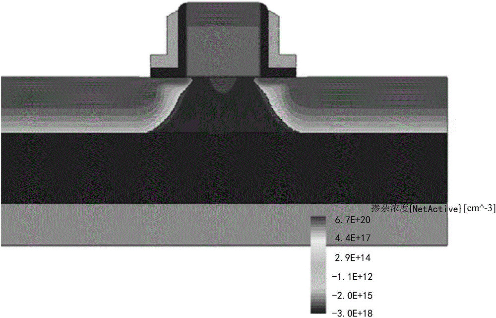
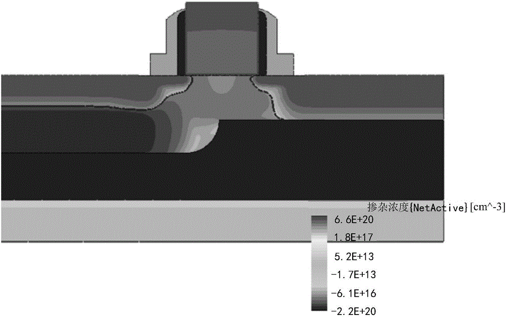
[0030] Such as Figure 7 As shown, an anti-single event transient hardened SOI device includes a substrate 1, a buried oxide layer 2, a semiconductor body region 3, a drain region 9, a source region 10, a gate region, a gate spacer 11, an LDD region 7 and a heavy The doped source extension region 8, the buried oxide layer 2 is located on the substrate 1, the material of the buried oxide layer 2 is silicon dioxide, and the semiconductor body region 3, the source region 10 and the drain region 9 are located between the buried oxide layer 2 , and the semiconductor body region 3 is located between the source region 10 and the drain region 9, the LDD region 7 is located at the top of both sides of the semiconductor body region 3 and is in contact with the source region 10 and the drain region 9 respectively, and the gate region is located at the top of th...


PUM


Abstract

The invention relates to the microelectronic technology field. The invention discloses an anti-single-event transient reinforcement SOI member, comprising a substrate, a buried oxide layer, a semiconductor body region, a drain region, a source region, a grid region, gridside walls, LDD regions and a heavily doped source extending region; the buried oxide layer is arranged above the substrate; the semiconductor body region, the source region and the drain region are arranged above the buried oxide layer; the semiconductor body region is positioned between the source region and the drain region; the LDD regions are positioned on two side ends of the semiconductor body region and in contact with the source region and the drain region; the grid region is positioned above the semiconductor body region; the two side gridside walls are arranged on two sides of the grid region and above the LDD regions; the source extending region is arranged among the source region, the semiconductor body region and the buried oxide layer; and the doping types of the source extending region and the source region are opposite. The invention also discloses a manufacture method for the anti-single-event transient reinforcement SOI member. The anti-single-event transient reinforcement SOI member and the manufacture method for the same can effectively inhibit SOI member single-event overturning and the single-event transient effect which are caused by single-event radiation, and the technology is simple and compatible with the current technology.

Description

technical field [0001] The invention belongs to the technical field of microelectronics, and in particular relates to an anti-single particle transient reinforced SOI device and a preparation method thereof. Background technique [0002] SOI (Silicon-on-Insulator) technology refers to the material preparation technology of forming a single crystal semiconductor silicon thin film layer with a certain thickness on the insulating layer and the process technology of manufacturing semiconductor devices on the thin film layer. SOI technology can realize full dielectric isolation of devices. Compared with bulk silicon technology isolated by PN junction, it has the advantages of no latch, high speed, low power consumption, high integration, high temperature resistance, and strong radiation resistance. It is widely used in high-speed, low power consumption, and radiation-resistant circuits. [0003] According to the thickness of SOI silicon film and the doping concentration and oper...

Claims


Application Information

Patent Timeline
Patent Type & Authority Applications(China)
IPC IPC(8): H01L21/762H01L27/12
CPCH01L21/7624H01L21/76264H01L27/1203
Inventor 黄辉祥耿莉韦素芬唐凯袁占生徐文斌吴一亮邱邑亮郑佳春
Owner JIMEI UNIV
Why Eureka
Try Eureka