Supercharge Your Innovation With Domain-Expert AI Agents!

System and method for testing off-chip driver impedance

A technology for testing circuits and drivers, which is applied in the direction of measuring resistance/reactance/impedance, measuring electrical variables, instruments, etc., and can solve problems such as difficulty in detecting through silicon vias 118

Active Publication Date: 2013-11-06
NAN YA TECH
View PDF6 Cites 2 Cited by
  • Summary
  • Abstract
  • Description
  • Claims
  • Application Information

AI Technical Summary

Problems solved by technology

Manufacturers typically probe the off-chip drivers of a given circuit (e.g., circuit 100) to test various characteristics (e.g., impedance), however, as TSV diameters decrease and pitches become narrower, making it more difficult to detect TSVs 118
Furthermore, testing the off-chip driver by connecting a test pad directly to the TSV 118 poses some problems, for example, the test pad can introduce considerable metal capacitance to the off-chip driver circuit (i.e., circuit 100)

Method used


Image

  • System and method for testing off-chip driver impedance
  • System and method for testing off-chip driver impedance
  • System and method for testing off-chip driver impedance

Examples


Embodiment Construction

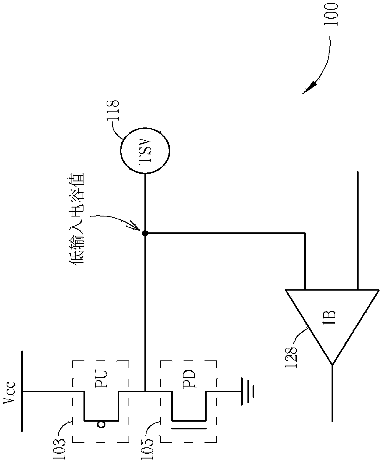
[0026] The invention discloses a test circuit and a test method, which can bring a relatively small capacitance value to the system when measuring the impedance of an off-chip driver coupled to a through-silicon via. In some embodiments, an OCD comparison test uses input buffers instead of directly connecting test pads to TSVs. In some cases, very little circuitry is added to the off-chip driver circuit in order to perform the off-chip driver comparison test or measure multiple off-chip drivers simultaneously.

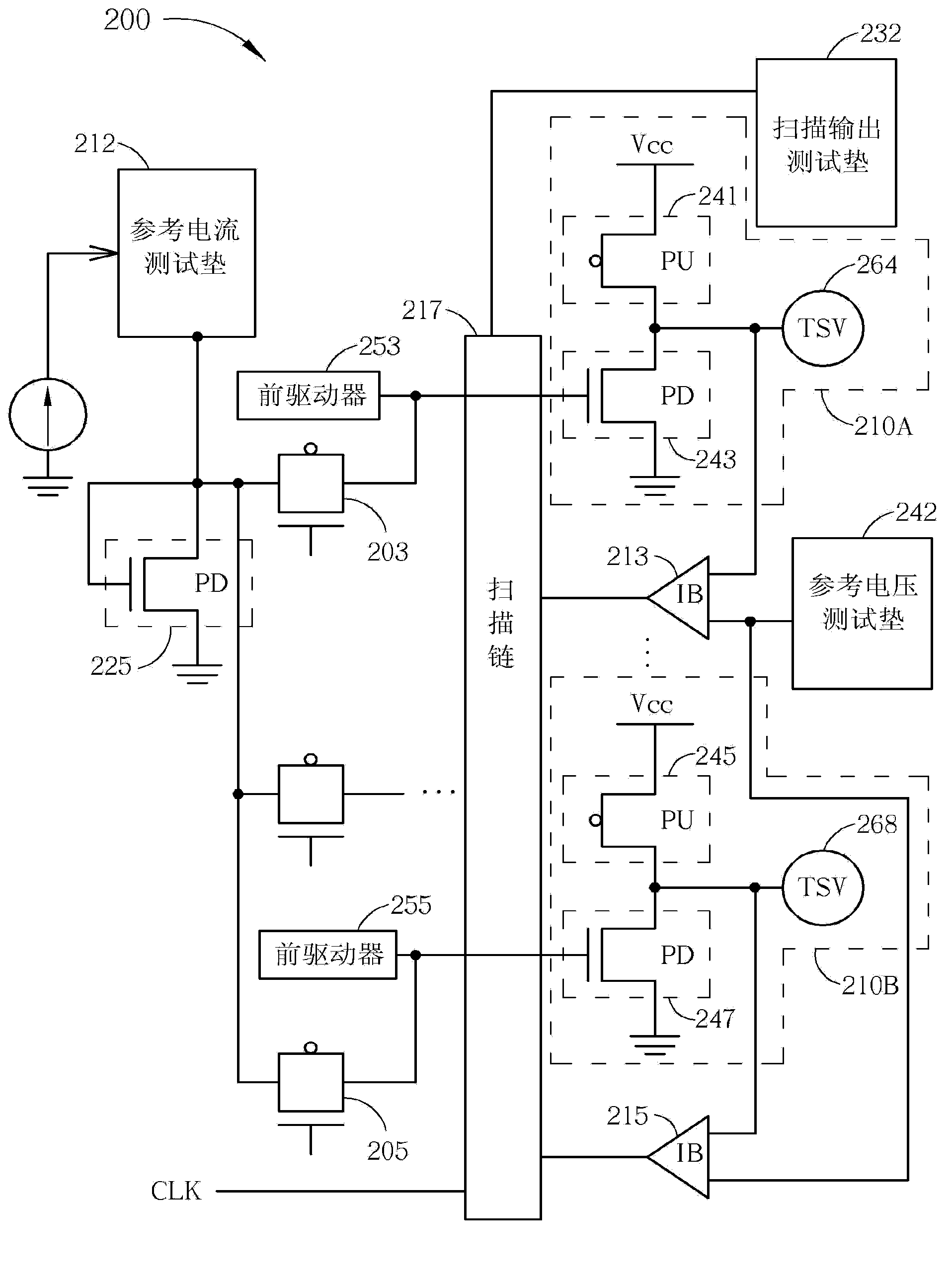
[0027] figure 2 is a schematic diagram of an embodiment of the test circuit 200 of the present invention. In the illustrated embodiment, the test circuit 200 includes a plurality of off-chip drivers 210A and 210B. The first off-chip driver 210A includes a first pull-up driver (in the present invention, interchangeable with a P-channel field effect transistor) 241 and a first pull-down driver (in the present invention, interchangeable with an N-channel field-effect t...


PUM


Abstract

A testing circuit for verifying the impedance of off-chip drivers includes: a plurality of off-chip drivers (OCD), each off-chip driver including a through-silicon via (TSV); an IREF test pad, for driving a current to the plurality of off-chip drivers; a plurality of pre-drivers, each respective pre-driver coupled to one of the plurality of off-chip drivers, wherein the plurality of pre-drivers are configured to turn on the off-chip drivers; a VREF test pad, for inputting a reference voltage to the testing circuit; a plurality of input buffers (IB) for outputting a plurality of comparison results, each of the plurality of input buffers configured to output the plurality of comparison results according to the reference voltage and the voltage at the TSV nodes; and a test pad, coupled to the plurality of IBs, for receiving the comparison results to determine whether the impedance of each OCD is within a desired range.

Description

technical field [0001] The invention relates to an off-chip driver, in particular to a system and method for testing the impedance of an off-chip driver using through-silicon holes. Background technique [0002] Semiconductor devices operate at specific operating voltages. As technology moves to sub-micron sizes and more and more operations are in the "low power" range, the accuracy of the operating voltage is critical for chip designers. become particularly important. An off-chip driver (OCD) is generally used to generate the aforementioned operating voltage to a semiconductor device (ie, a chip). Typically, off-chip interconnections are made through bond wires connected to bond pads on the chip. With the development of flip-chip technology and wafer stacking (wafer stacking) and other reasons, the driver chip interface has become more complex, thus requiring more complex bonding technology. Recently, an even bigger challenge for designers is to replace standard bond pad...

Claims


Application Information

Patent Timeline
Patent Type & Authority Applications(China)
IPC IPC(8): G01R27/14
CPCH03K19/00346H03K5/1534
Inventor 布雷特罗伯特·戴尔奥利弗·基尔
Owner NAN YA TECH
Features
  • R&D
  • Intellectual Property
  • Life Sciences
  • Materials
  • Tech Scout
  • Unparalleled Data Quality
  • Higher Quality Content
  • 60% Fewer Hallucinations
Learn More