Chip, chip connecting part, chip assembly, communication method of chip assembly, and printer

A technology for connecting parts and printers, applied in the field of imaging, can solve problems such as loss, inconvenience, and difficulty in troubleshooting for renters, and achieve the effect of avoiding abnormal work and avoiding losses.

Active Publication Date: 2013-11-13
ZHUHAI TIANWEI TECH DEV CO LTD
View PDF6 Cites 7 Cited by
  • Summary
  • Abstract
  • Description
  • Claims
  • Application Information

AI Technical Summary

Problems solved by technology

In this way, not only will it bring huge losses to the leaser, but the printer may also have printing failures due to compatibility issues. When maintaining the printer, it will bring difficulties and inconvenience to troubleshooting

Method used


Image

  • Chip, chip connecting part, chip assembly, communication method of chip assembly, and printer
  • Chip, chip connecting part, chip assembly, communication method of chip assembly, and printer
  • Chip, chip connecting part, chip assembly, communication method of chip assembly, and printer

Examples


no. 1 example

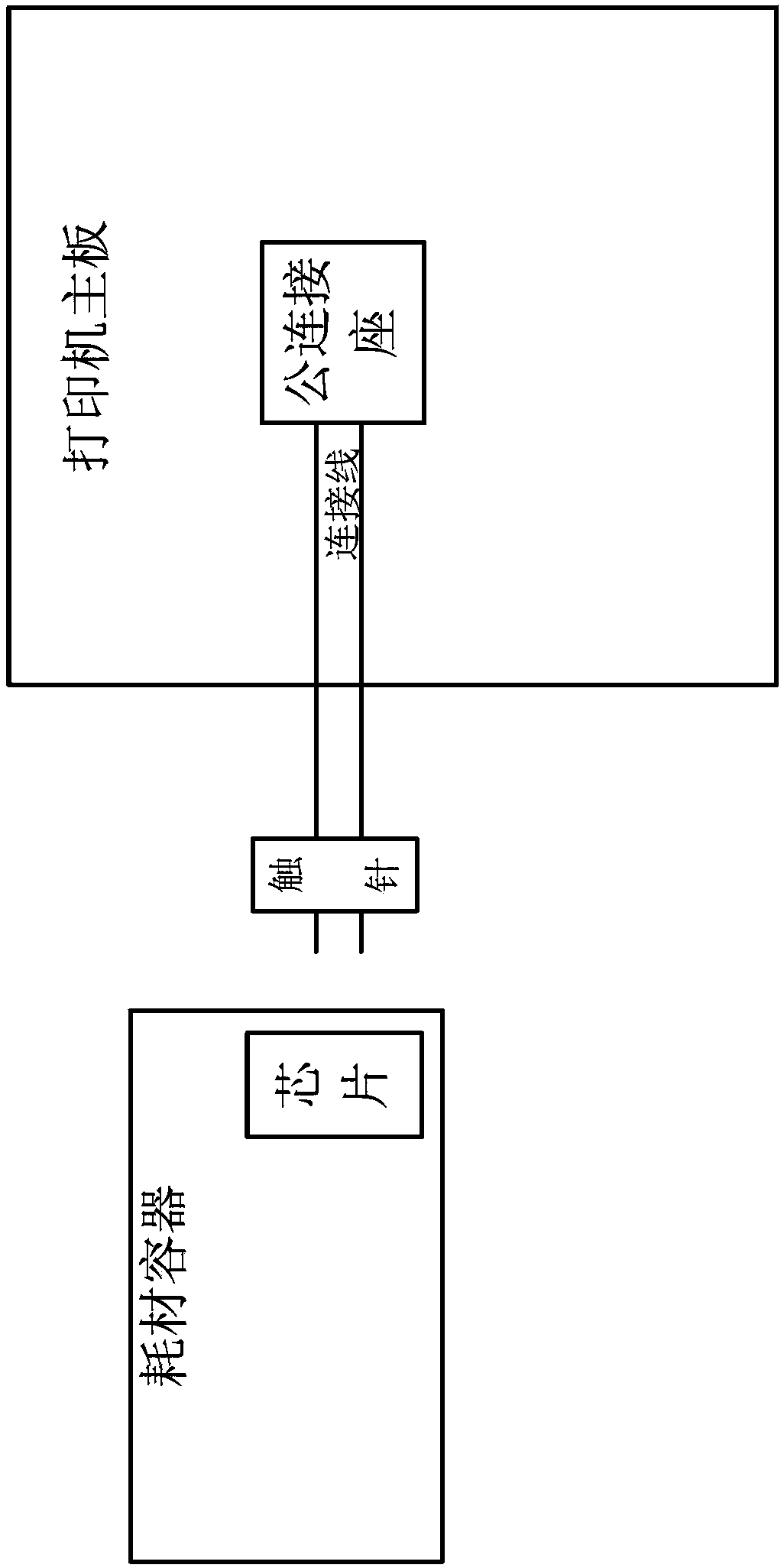
[0037] As another transformation of the first embodiment of the chip, the first embodiment of the chip connector and the first embodiment of the chip assembly of the present invention, the chip can be installed on the ink cartridge, and the chip connector is installed on the inkjet printer. At this time, The encryption memory of the chip and the storage unit of the chip connector store data related to the ink cartridge, and the rest of the structures and working principles are similar to those of this embodiment.

[0038] Second Embodiment of Chip, Chip Connector, and Chip Assembly

[0039] The chip provided in this embodiment is set on the toner cartridge. For the chip structure, see Image 6 ,Bag

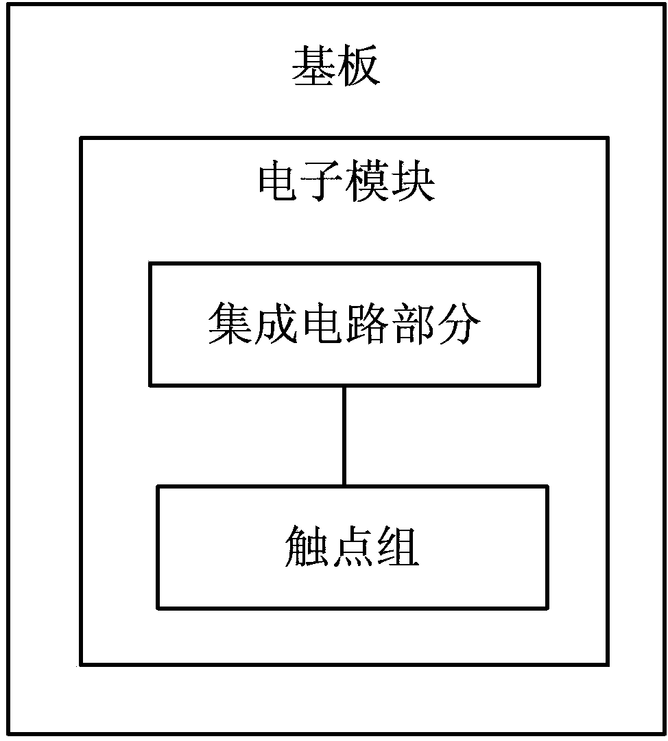
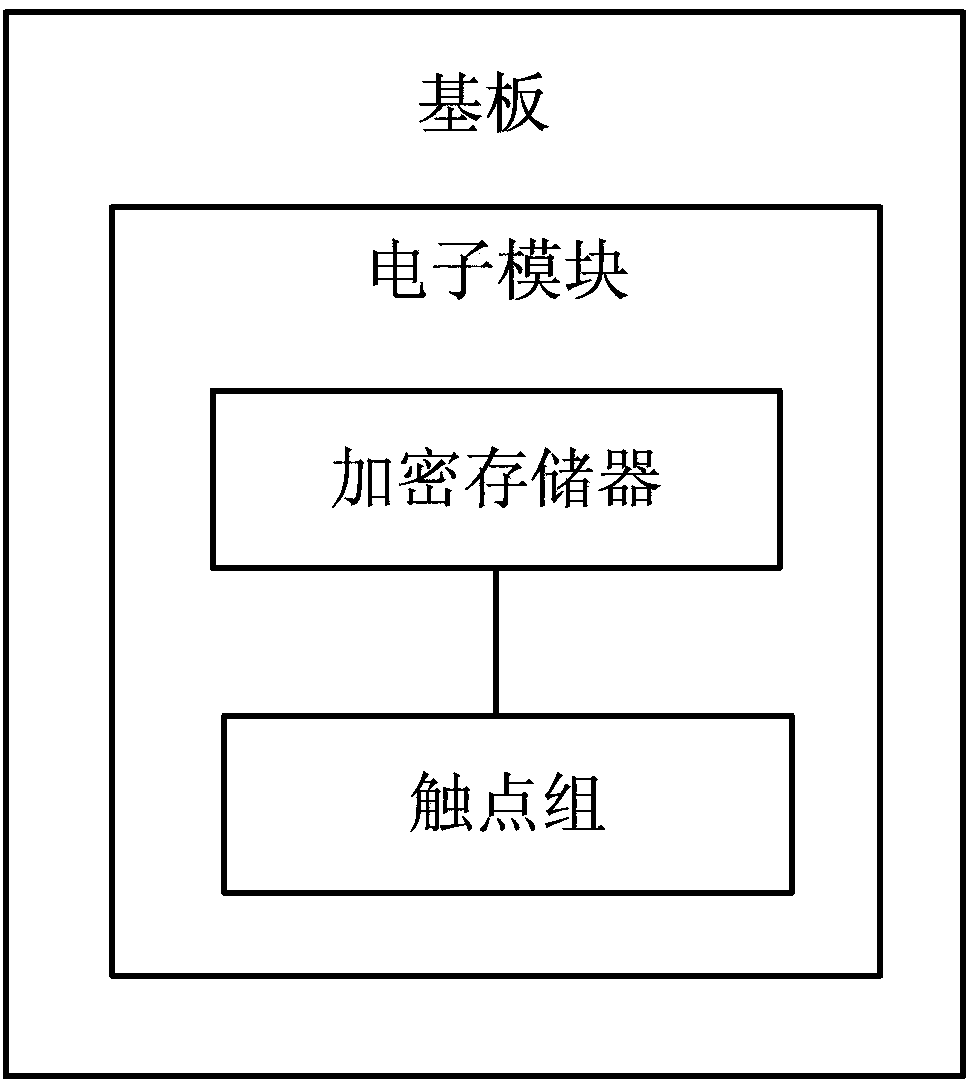
[0040] It includes a substrate and an electronic module installed on the substrate, the electronic module includes a contact group and a capacitor electrically connected to the contact group, and the contact group is used to connect with the contact pin.

[0041] The chip connec...

no. 2 example

[0048] As another transformation of the second embodiment of the chip, the second embodiment of the chip connector and the second embodiment of the chip assembly of the present invention, the chip can be installed on the ink cartridge, and the chip connector is installed on the inkjet printer. At this time, The encryption memory of the chip and the storage unit of the chip connector store data related to the ink cartridge, and the rest of the structures and working principles are similar to those of this embodiment.

[0049] Embodiment of chip component communication method

[0050] The structure of the chip component in this embodiment is as described in the above embodiment, and its communication method is: the chip connector first performs key authentication on the chip, if the chip passes the key authentication of the chip connector, the chip connector continues to judge whether the chip is Applicable to the chip connector, if the chip does not pass the key authentication ...


PUM


Abstract

The invention provides a chip installed on a consumable container. The chip comprises a substrate and an electronic module on the substrate, wherein the electronic module comprises a contact set and an electronic component electrically connected with the contact set, and the contact set is used for being connected with a contact pin; a chip connecting part comprises a connecting part substrate, an electronic module of the connecting part, a female through-connection part and a male through-connection part, the electronic module of the connecting part is installed on the connecting part substrate, the female through-connection part is used for being connected with a male connecting seat of a printer, the male through-connection part is used for guiding the contact pin out, the electronic module of the connecting part comprises an integrated circuit part electrically connected with the female through-connection part and the male through-connection part, the integrated circuit part comprises a storage unit and a control unit, the storage unit is used for storing measuring data and non-measuring data, and the control unit is connected with the storage unit to be used for achieving data communication between the chip connecting part and the chip, and between the chip connecting part and the printer. The invention further provides a chip assembly and a communication method of the chip assembly, and when the chip assembly and the communication method of the chip assembly are adopted, other people are prevented from using the chip and the consumable container unlawfully.

Description

technical field [0001] The invention relates to the field of imaging, in particular to a chip and its connectors, and a chip component, and also relates to a communication method and a printer for the chip component. Background technique [0002] The two commonly used printers are inkjet printers and laser printers. Inkjet printers use ink cartridges containing ink as consumable containers to provide printing ink to the printer to form text or patterns that need to be printed on paper; The toner cartridge with toner is used as a consumable container to provide the printer with toner for printing to form text or patterns that need to be printed on the medium. basically the same. The consumables containers mentioned in the present invention refer to ink cartridges and toner cartridges; the consumables mentioned in the present invention refer to ink or toner. [0003] With the widespread use of printers, more and more leasing companies provide free printers and matching paid ...

Claims


Application Information

Patent Timeline
Patent Type & Authority Applications(China)
IPC IPC(8): B41J2/175G03G15/08
Inventor 萧庆国谢立功
Owner ZHUHAI TIANWEI TECH DEV CO LTD
Why Eureka
Try Eureka