Low-voltage Bandgap voltage reference circuit and realizing method thereof

A voltage reference and circuit technology, which is applied in the field of low-voltage bandgap voltage reference circuits, can solve the problems of amplifier OP2 deviation and unfavorable applications, and achieve the effect of avoiding the offset being amplified

Active Publication Date: 2013-11-13
FAIRCHILD SEMICON SUZHOU
View PDF4 Cites 10 Cited by
  • Summary
  • Abstract
  • Description
  • Claims
  • Application Information

AI Technical Summary

Problems solved by technology

figure 2 In the Bandgap voltage reference circuit shown, the positive and negative input terminals of the op amp OP2 have the same voltage, and the resistance ratio of resistor R21 to resistor R23 is equal to the resistance ratio of resistor R22 to resistor R24. For example, resistor R21 can be two resistors R22 connected in series , the resistor R23 can be two resistors

Method used


Image

  • Low-voltage Bandgap voltage reference circuit and realizing method thereof
  • Low-voltage Bandgap voltage reference circuit and realizing method thereof
  • Low-voltage Bandgap voltage reference circuit and realizing method thereof

Examples


Embodiment Construction
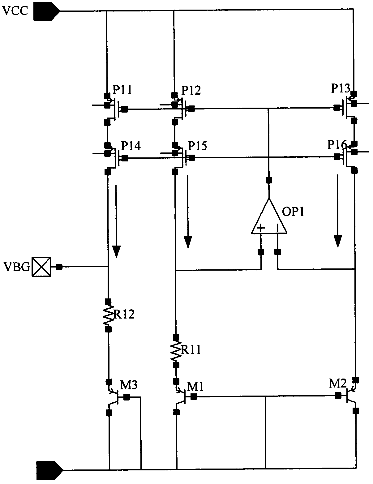
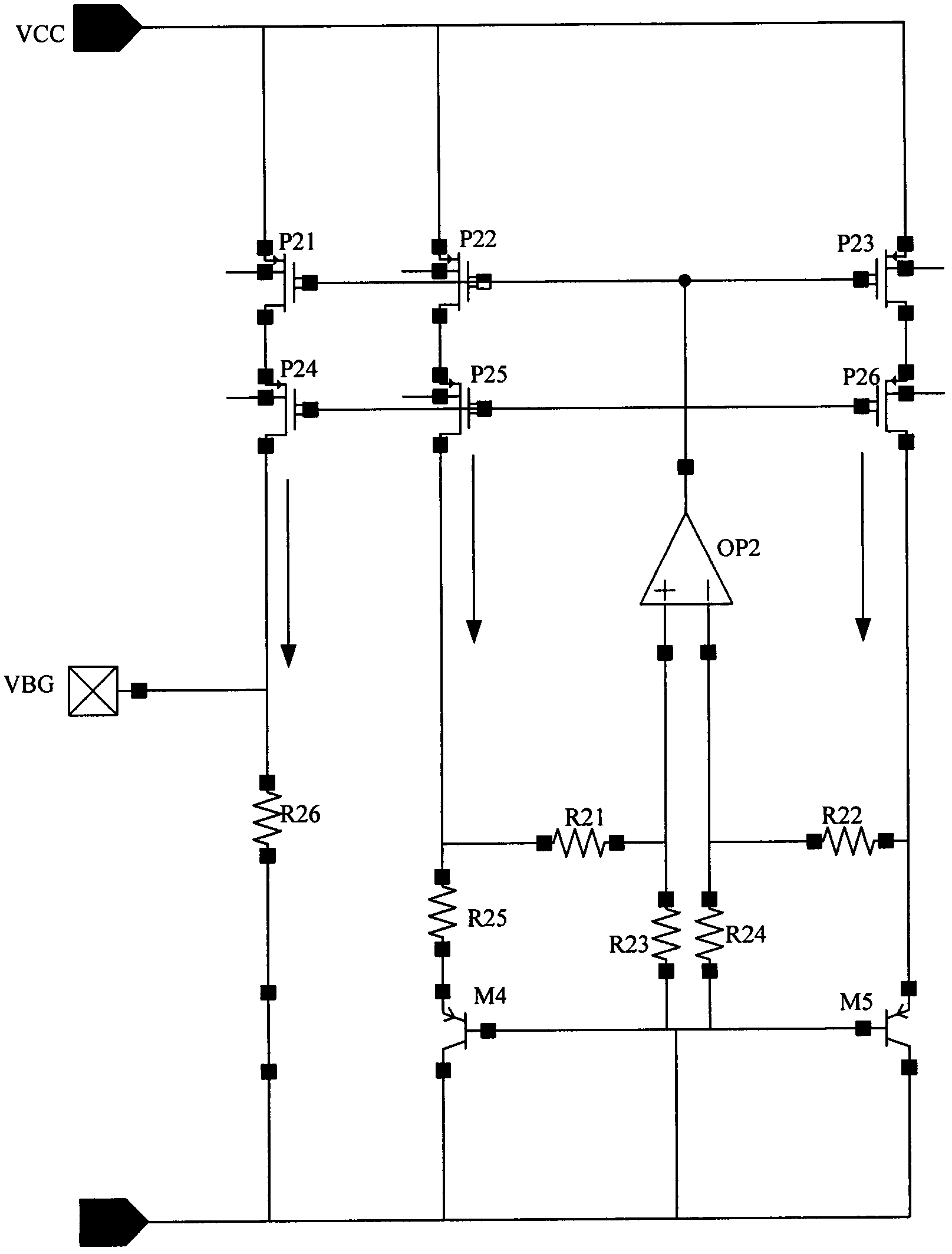
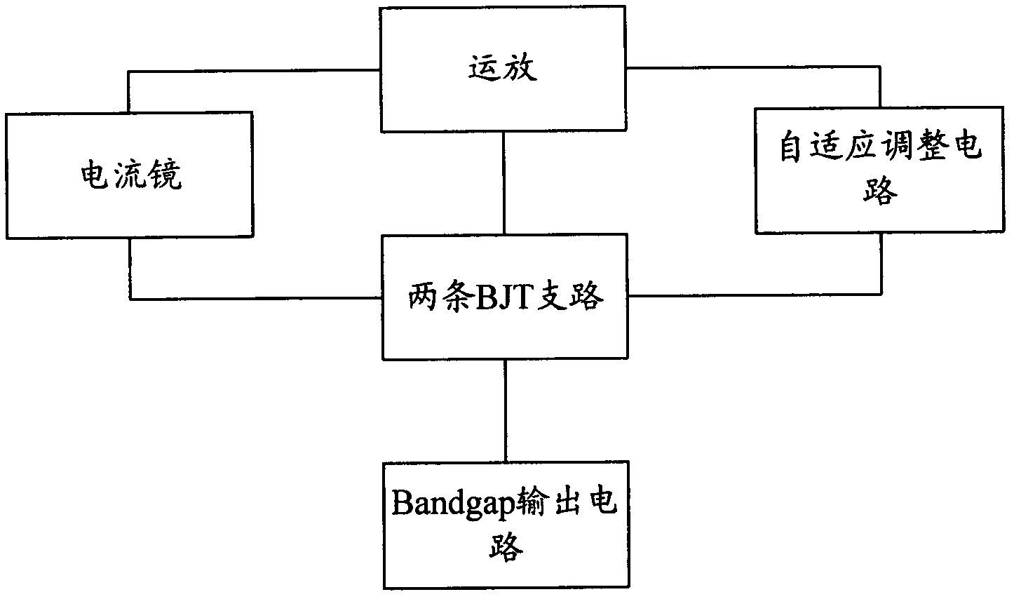
[0025] The basic idea of ​​the present invention is: input the voltage difference at the upper end of the two BJT branches to an operational amplifier adopting an NMOS input pair structure, the output end of the operational amplifier is connected to a current mirror, and use deep negative feedback to make the voltages at the upper end of the two BJT branches equal ; Adaptively adjust the base voltage of the common base BJT of the two BJT branches according to the working conditions of the NMOS input pair in the operational amplifier, control the current of the two BJT branch circuits, and ensure the normal operation of the operational amplifier.

[0026] The present invention will be further described in detail below with reference to the accompanying drawings and specific embodiments.

[0027] Embodiments of the present invention implement a low-voltage Bandgap voltage reference circuit, such as image 3 As shown, the circuit includes: a current mirror, an operational amplifi...


PUM


Abstract

The invention discloses a low-voltage Bandgap voltage reference circuit, which is characterized in that two BJT (Bipolar Junction Transistor) branches are differentially input to an operational amplifier adopting an NMOS (N-Mental-Oxide-Semiconductor) input pair structure; the output end of the operational amplifier is connected to a current mirror, and voltages on the two BJT branches are enabled to be equal by utilizing deep negative feedback; the base voltage of a shared base BJT in the two BJT branches are adjusted in a self-adaptive mode according to the work conditions of NMOS input pair in the operational amplifier, so currents of the two BJT branches are controlled, and the operational amplifier is enabled to normally work; and the output voltage of the Bandgap voltage reference circuit is generated in a mirror image mode. The invention also discloses a realizing method of the low-voltage Bandgap voltage reference circuit, through the scheme disclosed by the invention, the input voltage of the Bandgap voltage reference circuit is reduced, the Bandgap voltage reference circuit is enabled to work under the lower input voltage, and the deviation of the operational amplifier is prevented from being amplified.

Description

technical field [0001] The invention relates to voltage reference source technology, in particular to a low-voltage bandgap (Bandgap) voltage reference circuit and a realization method thereof. Background technique [0002] As a basic unit circuit, the voltage reference source plays an extremely important role in circuits such as digital / analog (D / A), analog / digital (A / D) converters and SDRAM. Among many types of voltage reference sources, the Bandgap voltage reference circuit is the most widely used. [0003] Traditional Bandgap voltage reference circuits generally have figure 1 and figure 2 The two structures shown, figure 1 Among them, P-type-metal-oxide-semiconductor (PMOS, P-Mental-Oxide-Semiconductor) P11, PMOS P12, and PMOS P13 constitute a cascode current mirror, which is used to mirror the current on each other's circuits, and PMOS P14, PMOS P15 and PMOS P16 form a cascode circuit. The positive input terminal of the operational amplifier (hereinafter referred t...

Claims


Application Information

Patent Timeline
IPC IPC(8): G05F1/56
CPCG05F3/02G05F3/30
Inventor 黄雷
Owner FAIRCHILD SEMICON SUZHOU
Why Eureka
Try Eureka