
Rail-to-rail-input buffer

a buffer and rail technology, applied in the direction of dc-amplifiers with dc-coupled stages, different amplifiers, semiconductor devices/discharge tubes, etc., can solve the problems of unbalanced summer in the high common mode operation region, signal contributes to additional noise, clock signal not necessarily available in a linear system, etc., to reduce distortion at the extremes of the input voltage range and the effect of distortion

Inactive Publication Date: 2007-01-02
INFINEON TECH AG
View PDF10 Cites 13 Cited by
  • Summary
  • Abstract
  • Description
  • Claims
  • Application Information

AI Technical Summary

Benefits of technology

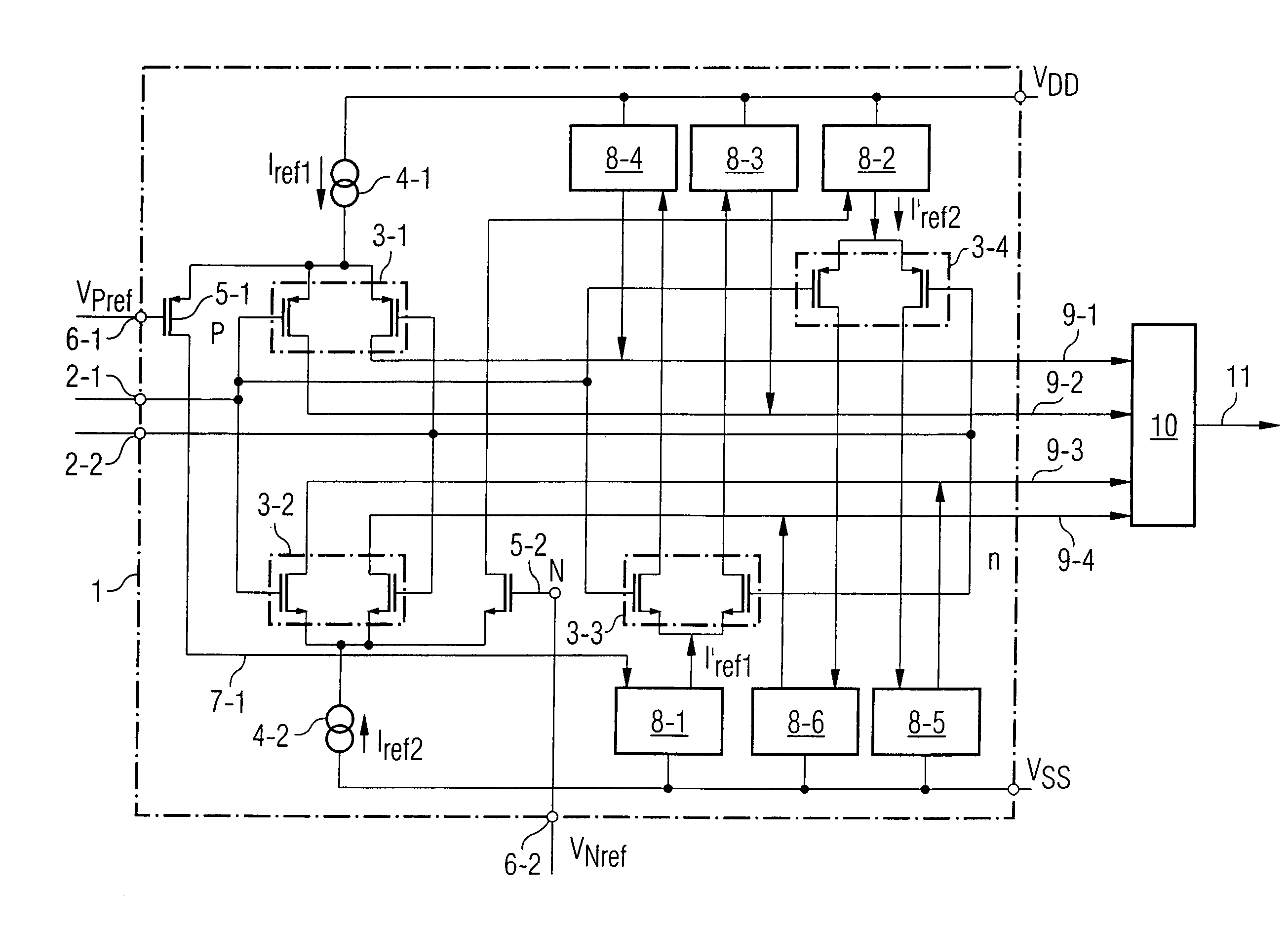
[0027]A first advantage of the rail-to-rail-input buffer according to the present invention resides in that it provides a proportional, related to the input voltage, push-pull output current drive through the summer over the full rail-to-rail-input signal range. Consequently distortion at the extremes of the input voltage range is reduced.
[0028]A second advantage of the rail-to-rail input buffer according to the present invention is that a fixed DC biasing is maintained to the output summer over the whole input signal range. Thus the distortion at extremes of the input voltage is lowered.
[0039]The provision of the third, fourth, fifth and sixth current mirror circuit has the advantage that the summer connected to the rail-to-rail-input buffer is driven symmetrically. This gives a proportional, related to the input voltage, push-pull output current drive to the summer circuit over the full rail-to-rail-input signal range. This helps to reduce distortion at extremes of the input voltage range.

Problems solved by technology

A clock signal is not necessarily available in a linear system.
Further a clock signal contributes to additional noise.
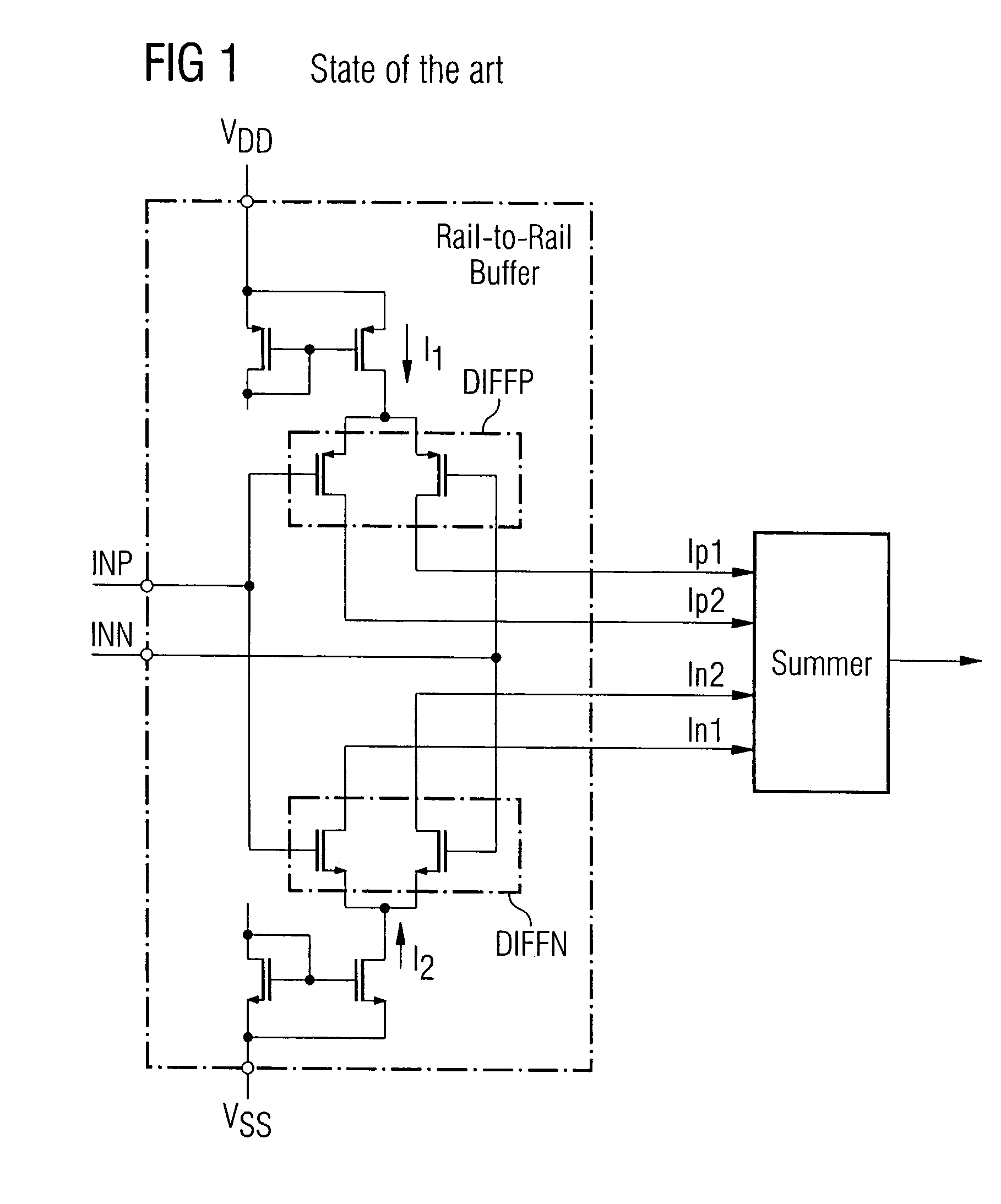
A further disadvantage of the rail-to-rail buffer according to the state of the art as shown in FIG. 1 is that the summer is driven unbalanced in the high common mode operation region and in the low common mode operation region of the rail-to-rail buffer.
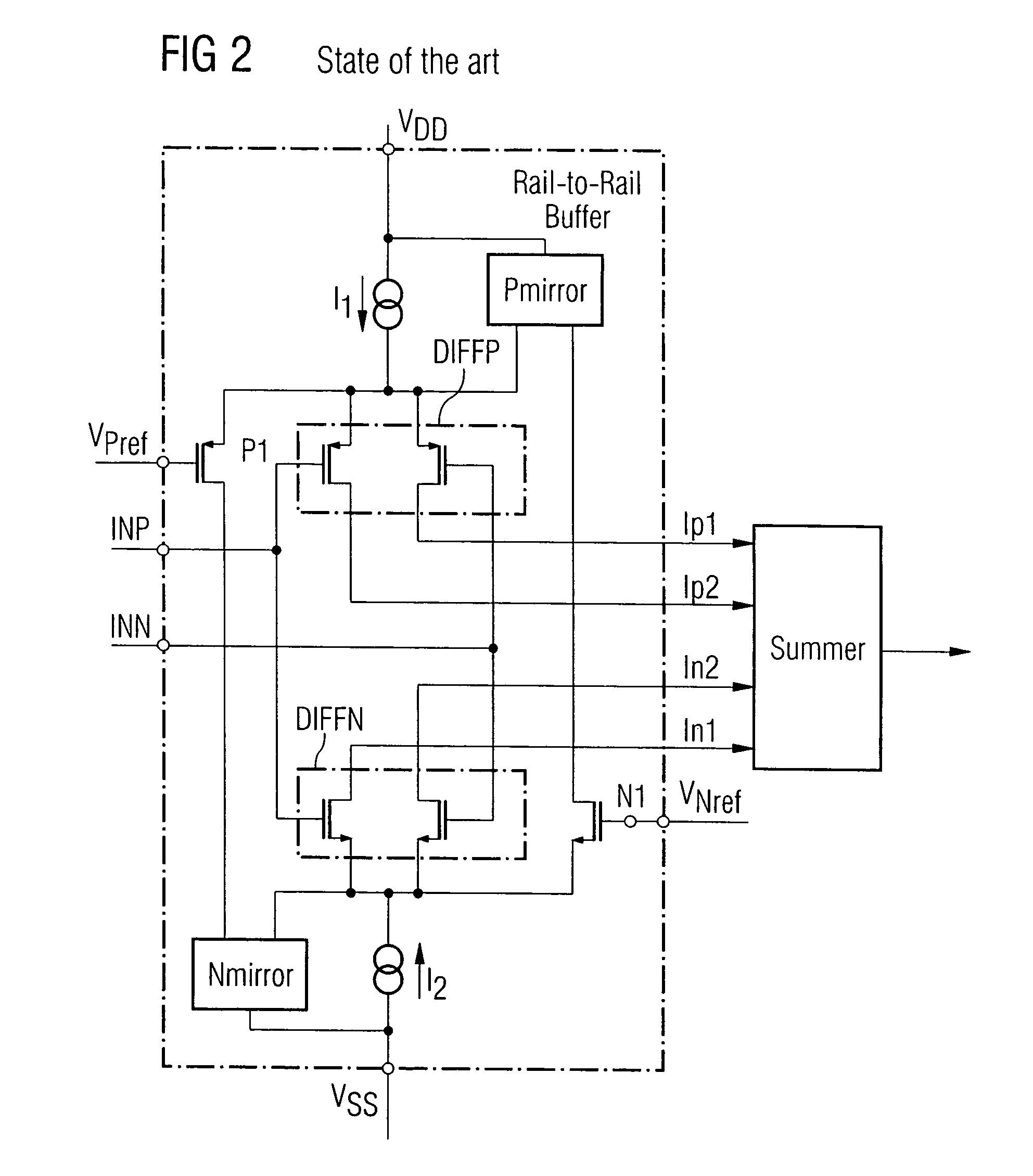
The rail-to-rail buffer according to the state of the art as shown in FIG. 2 has as a primary disadvantage that it relies on long-channel devices, e.g. long-channel MOS-transistors within the differential stages DIFFP and DIFFN.
Accordingly a rail-to-rail buffer having small dimensions will not provide a constant mutual conductance gm over the full input signal range.
A secondary disadvantage of the rail-to-rail buffer as shown in FIG. 2 is in that the summer is driven unbalanced in the high and low common mode operation regions.

Method used


Image

  • Rail-to-rail-input buffer
  • Rail-to-rail-input buffer
  • Rail-to-rail-input buffer

Examples


Embodiment Construction

[0047]As can be seen from FIG. 3 the rail-to-rail-input buffer 1 according to the present invention has a differential input having a first input terminal 2-1 and a second input terminal 2-2 for supplying an input signal.

[0048]A first differential stage 3-1 is supplied with a first reference current Iref1 which is generated by a first reference current source 4-1. The first differential stage 3-1 is formed by two PMOS-transistors having gate terminals which are connected to the input terminals 2-1, 2-2.

[0049]The rail-to-rail-input buffer 1 comprises a second differential stage 3-2 supplied with a second reference current Iref2 generated by a second reference current source 4-2. The second differential stage 3-2 is formed by two NMOS-transistors having gate terminals which are connected to the input terminals 2-1, 2-2 of the rail-to-rail-input buffer 1.

[0050]The rail-to-rail-input buffer 1 further comprises a first switching transistor 5-1 and a second switching transistor 5-2 in the...


PUM


Abstract

A rail-to-rail-Input Buffer with constant mutual conductance includes a differential input; a first differential stage supplied with a first reference current; a second differential stage supplied with a second reference current; a switching PMOS-transistor which switches through when the input signal is higher than a first threshold voltage to divert the first reference current to a first current mirror circuit; a switching NMOS-transistor which switches through when an input signal is lower than a second threshold voltage to divert the second reference current to a second current mirror circuit; a third differential stage supplied with the mirrored first reference current and replaces the first differential stage when the input signal is higher than the first threshold voltage; and a fourth differential stage supplied with the mirrored second reference current and replaces the second differential stage when the input signal is lower than the second threshold voltage.

Description

FIELD OF THE INVENTION[0001]The invention relates to a rail-to-rail-input buffer with constant mutual conductance having a composite P and N channel differential input pair.BACKGROUND OF THE INVENTION[0002]In many baseband applications a buffer / amplifier is required which possesses linear operation over an input signal range which extends across the full range of the supply voltage. These buffer / amplifiers are referred to as rail-to-rail-input buffers.[0003]There are two basic types of conventional rail-to-rail-input buffers. In the first type a local high voltage on chip is used to drive a conventional differential input stage. This first type requires a charge pump and a clock signal. A clock signal is not necessarily available in a linear system. Further a clock signal contributes to additional noise.[0004]A second type of rail-to-rail-input buffers use a composite P and N channel differential input pair. Composite N and P channel differential input pairs exist in a number of var...

Claims


Application Information

Patent Timeline
Patent Type & Authority Patents(United States)
IPC IPC(8): H03F3/45
CPCH03F3/45112
Inventor DAWES, ALAN
Owner INFINEON TECH AG
Learn More