
MEMS microphone structure and manufacturing method thereof

A manufacturing method and microphone technology, which are applied to electrostatic transducer microphones, sensors, electrical components, etc., can solve the problems of complex manufacturing process and packaging process, high cost, bulky volume, etc., and achieve the effect of improving anti-interference ability.

Active Publication Date: 2013-11-13
MEMSEN ELECTRONICS
View PDF3 Cites 9 Cited by
  • Summary
  • Abstract
  • Description
  • Claims
  • Application Information

AI Technical Summary

Problems solved by technology

Moreover, the manufacturing process and packaging process of this MEMS packaging structure are complex, bulky and costly.

Method used


Image

  • MEMS microphone structure and manufacturing method thereof
  • MEMS microphone structure and manufacturing method thereof
  • MEMS microphone structure and manufacturing method thereof

Examples


Embodiment 1

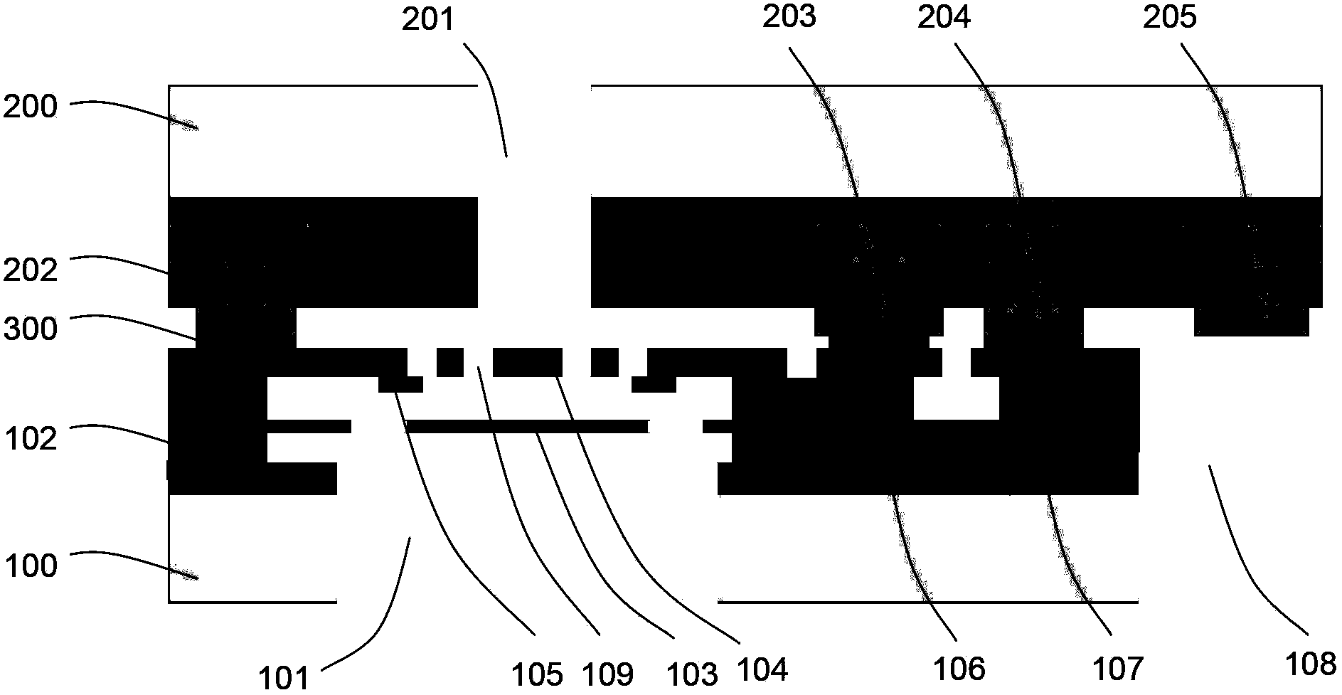
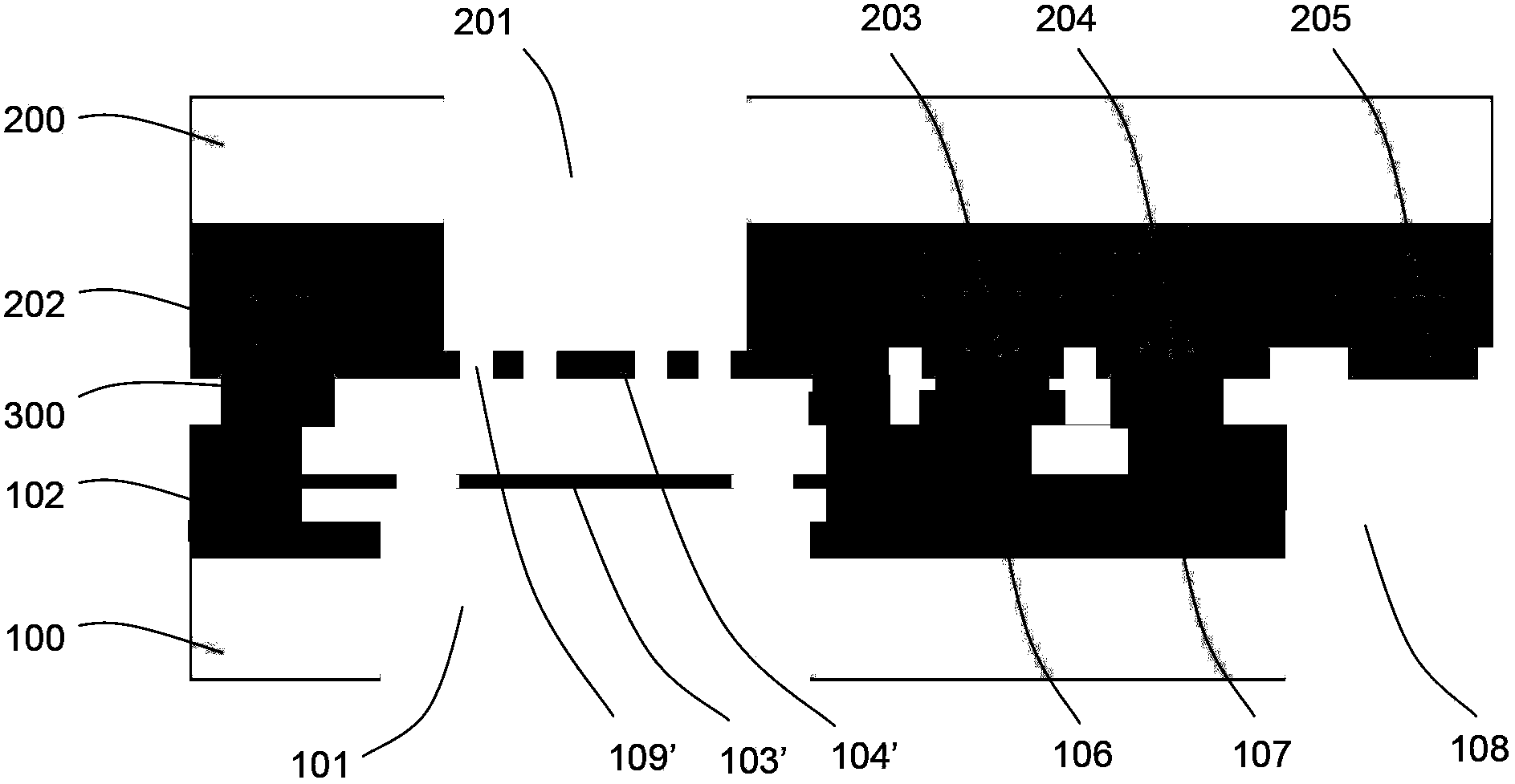
[0045] For the MEMS microphone structure of this embodiment, please refer to figure 1 ,include:

[0046] A first substrate 100, the first substrate has a first opening 101;

[0047]The first dielectric layer 102 and the first conductive structure layer on the first substrate 100, the first conductive structure layer includes a MEMS microphone assembly, a first conductive adhesive structure 106, and a first substrate conductive structure 107, wherein , the MEMS microphone assembly includes a sensitive film 103 and a fixed electrode 104 corresponding to the sensitive film 103, the first opening 101 corresponds to the sensitive film; the upper surface of the first conductive adhesive structure 106 is the first bonding surface; the first substrate conductive structure 107 penetrates through the first dielectric layer 102 and is connected to the first substrate 100;

[0048] The second substrate 200, the second substrate contains signal processing circuit elements ( figure 1 no...

Embodiment 2

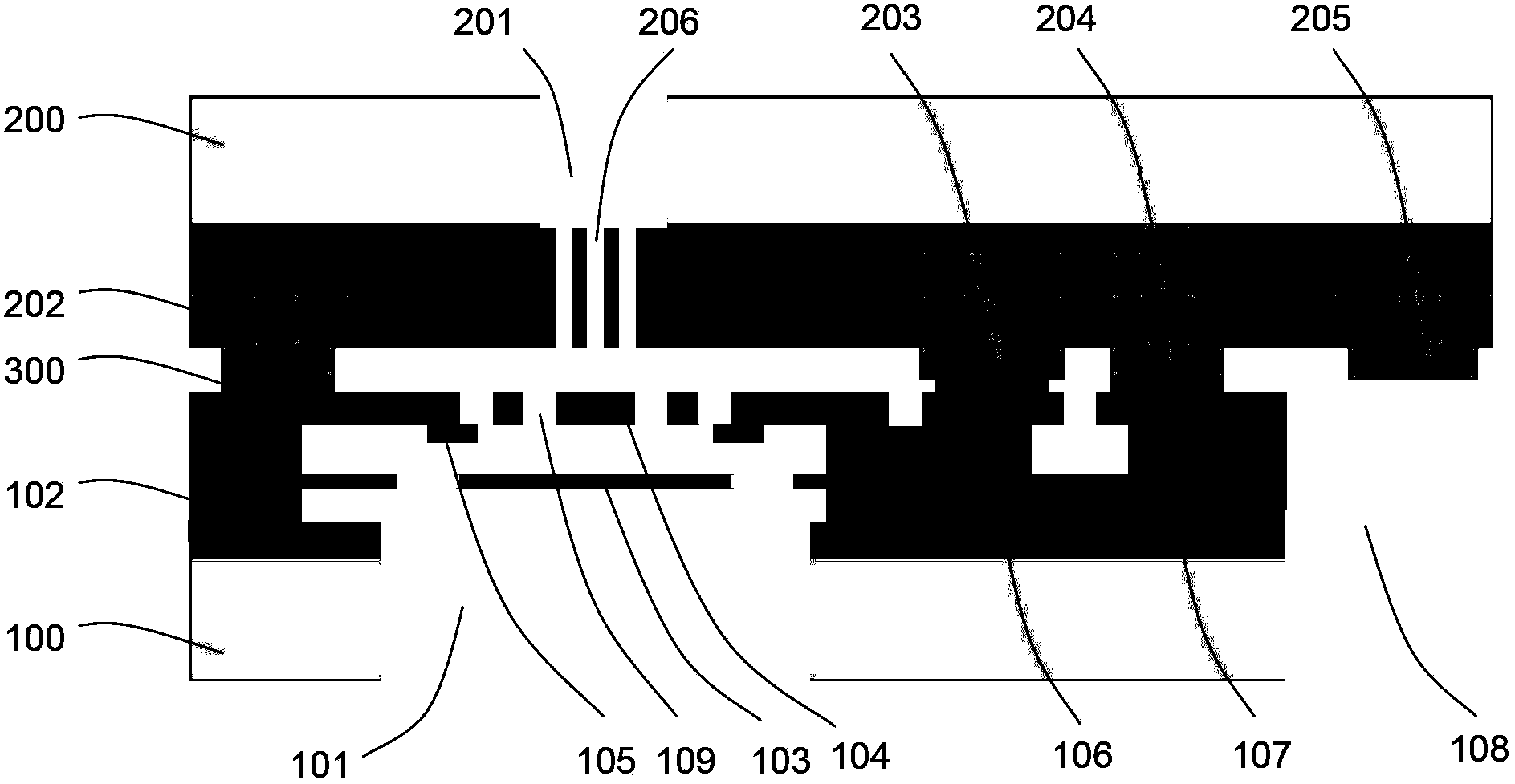
[0063] For the MEMS microphone structure of this embodiment, please refer to image 3 The difference between this embodiment and Embodiment 1 is that there is at least one through hole in the second dielectric layer 202 corresponding to the sensitive film 103 of the MEMS microphone component or the fixed electrode 104 corresponding to the sensitive film 103 206 , the second opening 201 of the second substrate 200 exposes the sensitive film 103 or the fixed electrode 104 through the through hole 206 . Other parts of the structure of the MEMS microphone in this embodiment are identical to those in Embodiment 1, and will not be repeated here.

[0064] In this embodiment, there is at least one through hole 206 in the second dielectric layer 202 corresponding to the sensitive film 103 or the fixed electrode 104 of the MEMS microphone assembly, so that a hole 206 remains above the sensitive film 103 or the fixed electrode 104. Part of the second dielectric layer, forming such a str...

Embodiment 3

[0067] On the basis of Embodiment 2, the MEMS microphone structure in this embodiment also includes a third conductive structure, see Figure 5 The difference between this embodiment and the second embodiment is that: there is a third conductive structure 207 in the second dielectric layer 202 corresponding to the sensitive film 103 of the MEMS microphone component or the fixed electrode 104 corresponding to the sensitive film 103 and at least one through hole 206 ′, the through hole 206 ′ passes through the second dielectric layer 202 and the third conductive structure 207 . Other parts of the MEMS microphone structure of the present embodiment are the same as those of the second embodiment ( image 3 ) are exactly the same and will not be repeated here.

[0068] Preferably, the third conductive structure is layered, and one or more surfaces of the layered third conductive structure are covered by the second dielectric layer, Figure 5 In the above, the third conductive str...


PUM


Abstract

The invention provides an MEMS microphone structure and a manufacturing method thereof. According to the MEMS microphone structure, a second conducting structure layer and a first conducting structure layer are attached through a first conducting adhered structure and a second conducting adhered structure in a face-to-face mode, wherein the second conducting structure layer and a second substrate jointly form a signal processing circuit, the first conducting structure layer is arranged on a first substrate provided with an MEMS microphone assembly, the first conducting structure layer comprises a first substrate conducting structure connected with the first substrate, and the second conducting structure layer comprises a second substrate conducting structure connected with the second substrate. Through the adoption of the MEMS microphone structure, when the EMS microphone assembly operates, the first substrate conducting structure and / or the second substrate conducting structure are / is connected with a ground potential or in ground connection through low impedance or connected with other screen potentials, external electric interference can be shielded, and antijamming capability of the MEMS microphone structure is improved.

Description

technical field [0001] The invention relates to a micro-electromechanical system technology, in particular to a MEMS microphone structure and a manufacturing method thereof. Background technique [0002] MEMS (Micro-Electro-Mechanical Systems, Micro-Electro-Mechanical Systems) microphones using Micro-Electro-Mechanical Systems technology have become an alternative to Electret Condenser Microphones (ECM) using organic membranes due to their miniaturization and lightness. One of the top candidates. [0003] MEMS microphones are miniature microphones made by etching pressure-sensing diaphragms on semiconductors through micro-electro-mechanical systems technology. They are commonly used in mobile phones, earphones, laptops, cameras and cars. Driven by the need for MEMS microphones to be compatible with CMOS and the further reduction in the size of MEMS microphones, the packaging structure of MEMS microphones has become a research hotspot. Many companies have invested a lot of m...

Claims


Application Information

Patent Timeline
IPC IPC(8): H04R19/04H04R31/00
Inventor 柳连俊
Owner MEMSEN ELECTRONICS
Learn More