Pixel and pixel circuit

A pixel circuit and pixel technology, applied in circuits, electric light sources, electrical components, etc., can solve problems such as aging of light-emitting diodes, decrease in pixel aperture ratio, and no solutions have been developed.

Active Publication Date: 2013-11-20
AU OPTRONICS CORP
View PDF5 Cites 14 Cited by
  • Summary
  • Abstract
  • Description
  • Claims
  • Application Information

AI Technical Summary

Problems solved by technology

[0002] In the display panel, in order to effectively control the light-emitting diodes in the pixels, a pixel circuit is usually configured. However, the display panel using the pixel circuit will face many problems, such as transistor variation, voltage drop (IR drop), light-emitting diode aging, etc. The above-mentioned problems will lead to uneven brightness of the display panel, which will degrade the image quality of the display panel.
[0003] Although a compensation circuit can be arranged in the pixel to improve various defects caused by the above problems, however, if a large number of transistors are arranged in the compensation circuit, problems such as a decrease in the pixel aperture ratio and limited resolution will be derived
[0004] This shows that above-mentioned existing mode obviously still has inconvenience and defective, and needs to be improved
In order to solve the above problems, related fields have tried their best to find a solution, but a suitable solution has not been developed for a long time.

Method used


Image

  • Pixel and pixel circuit
  • Pixel and pixel circuit
  • Pixel and pixel circuit

Examples


Embodiment Construction

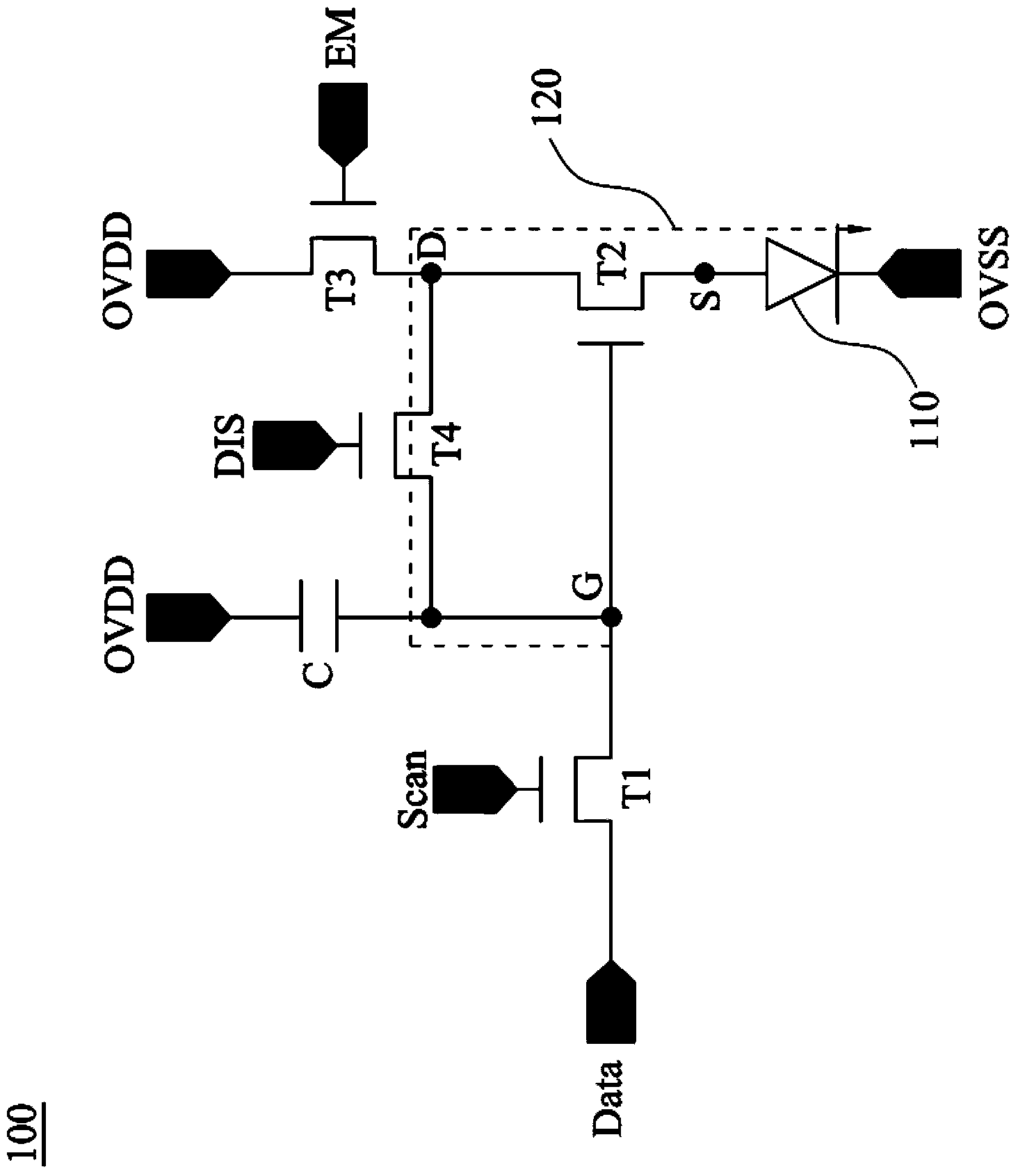
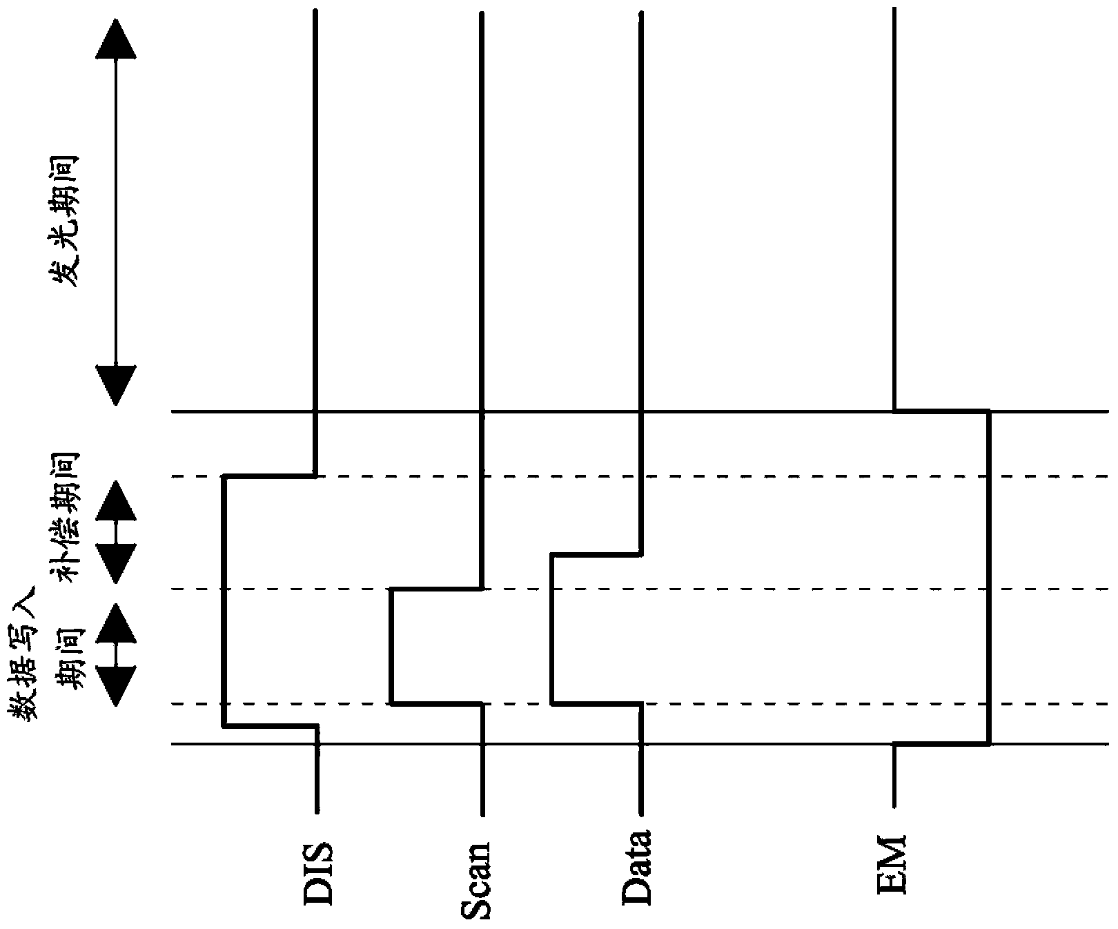
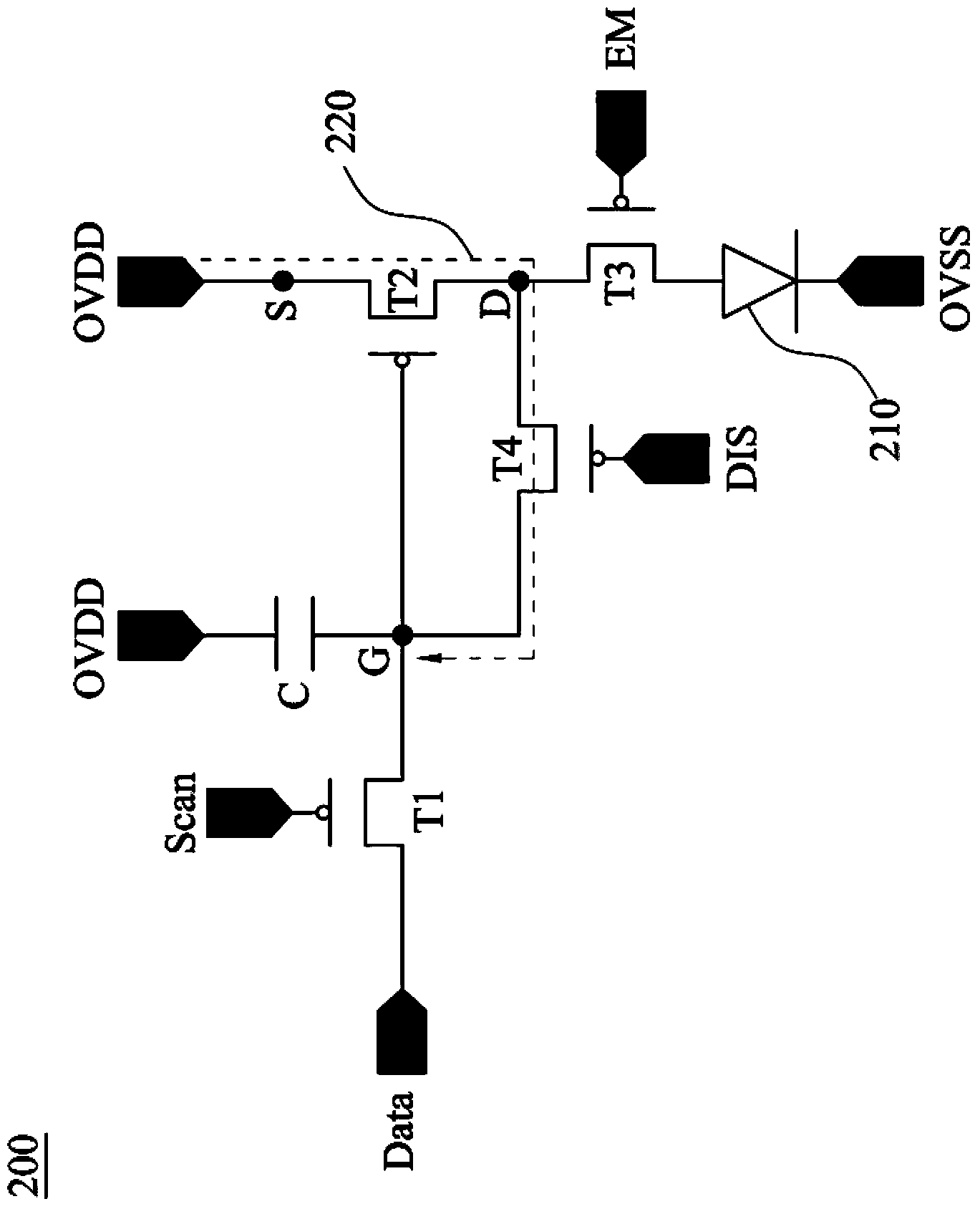
[0037] In order to make the description of the present disclosure more detailed and complete, the following provides an illustrative description of the implementation aspects and specific embodiments of the present invention; but this is not the only form of implementing or using the specific embodiments of the present invention. The description covers features of various embodiments as well as method steps and their sequences for constructing and operating those embodiments. However, other specific embodiments can also be used to achieve the same or equivalent functions and step sequences.

[0038] Unless otherwise defined in this specification, the meanings of scientific and technical terms used herein are the same as those commonly understood and commonly used by those skilled in the art to which this invention belongs. In addition, the singular nouns used in this specification include the plural forms of the nouns, and the plural nouns used also include the singular forms ...


PUM


Abstract

Disclosed are a pixel and a pixel circuit. The pixel comprises an organic light emitting diode, a drive transistor, a first switch, a third switch, and a fourth switch. The drive transistor is electrically coupled to the organic light emitting diode. When the pixel is in a data writing period, the first switch is employed to write data voltage into a control terminal of the drive transistor. When the pixel is in a compensation period, the fourth switch enables the conduction of the control terminal and a first terminal of the drive transistor so as to enable the control terminal of the drive transistor to charge and discharge through a current path and enable voltage of the control terminal of the drive transistor to form compensation voltage. The compensation voltage enables the conduction of the drive transistor during a light emitting period, and the third switch is turned on so as to enable drive current to be supplied to the organic light emitting diode. In addition, the pixel circuit is also disclosed.

Description

technical field [0001] The present invention relates to a basic electronic circuit, in particular to a pixel and its circuit. Background technique [0002] In the display panel, in order to effectively control the light-emitting diodes in the pixels, a pixel circuit is usually configured. However, the display panel using the pixel circuit will face many problems, such as transistor variation, voltage drop (IR drop), light-emitting diode aging, etc. The above-mentioned problems will lead to uneven brightness of the display panel, which will degrade the image quality of the display panel. [0003] Although the compensation circuit can be arranged in the pixel to improve various defects caused by the above-mentioned problems, however, if a large number of transistors are arranged in the compensation circuit, problems such as decreased aperture ratio of the pixel and limited resolution will be derived. [0004] This shows that above-mentioned existing mode obviously still has i...

Claims


Application Information

Patent Timeline
Patent Type & Authority Applications(China)
IPC IPC(8): G09G3/32H01L27/32H05B44/00
CPCG09G2300/0814G09G2300/0819G09G2320/0233G09G2320/045G09G3/3233
Inventor 刘立伟许文曲
Owner AU OPTRONICS CORP
Why Eureka
Try Eureka