CMOS TDI image sensor and charge transfer control method thereof

An image sensor and charge transfer technology, applied in image communication, television, electrical components, etc., can solve the problem of reducing image quality and achieve the effect of improving image resolution

Active Publication Date: 2013-11-20
GPIXEL
View PDF5 Cites 21 Cited by
  • Summary
  • Abstract
  • Description
  • Claims
  • Application Information

AI Technical Summary

Problems solved by technology

The biggest disadvantage of this kind of image sensor is that the voltage addition must be completed through the circuit, so that each addition will introduce new circuit noise and reduce the image quality

Method used


Image

  • CMOS TDI image sensor and charge transfer control method thereof
  • CMOS TDI image sensor and charge transfer control method thereof
  • CMOS TDI image sensor and charge transfer control method thereof

Examples


Embodiment 1

[0055] The case of n=3, m=2, i=1 (the area of ​​the pixel area is 3x3 area of ​​the charge collection unit). The combined number of charge transfer channels is 3.

[0056] like Figure 13 As shown, the dotted box indicates the charge storage area (ie, the charge collection area), and the obliquely shaded area indicates the pixel area (the area of ​​the pixel area is 3×3). like Figure 14 As shown, the charge in the charge collection area is represented by the black solid line, and the pixel charge in other areas is represented by the gray solid line)

[0057] At time t1, the area of ​​the charge storage area is 3×2; at time t2, the area of ​​the charge storage area is 3×1; at time t3, the area of ​​the charge storage area is 3×2; at time t4, the area of ​​the charge storage area is 3× 1;....... At equal intervals, the area of ​​the charge storage region changes from 3x2 to 3x1 or from 3x1 to 3x2. Every two equal time intervals, the charge storage region moves one charge t...

Embodiment 2

[0059] n=4, m=3, i=2 case (the area of ​​the pixel area is 4x4 area of ​​the charge collection unit). The combined number of charge transfer channels is 4.

[0060] like Figure 15 As shown, the dotted line box represents the charge storage area (that is, the charge collection area), and the obliquely shaded area represents the pixel area (the area of ​​the pixel area is 4×4). like Figure 16 As shown, the charge in the charge collection area is represented by the black solid line, and the pixel charge in other areas is represented by the gray solid line)

[0061] At time t1, the area of ​​the charge storage area is 4×3; at time t2, the area of ​​the charge storage area is 4×2; at time t3, the area of ​​the charge storage area is 4×3; at time t4, the area of ​​the charge storage area is 4× 2;....... At equal intervals, the area of ​​the charge storage region changes from 4x3 to 4x2 or from 4x2 to 4x3. Every two equal time intervals, the charge storage region moves one cha...

Embodiment 3

[0063] The case of n=4, m=3, i=1 (the area of ​​the pixel area is 4x4 area of ​​the charge collection unit). The combined number of charge transfer channels is 4.

[0064] like Figure 17 As shown, the dotted line box represents the charge storage area (that is, the charge collection area), and the obliquely shaded area represents the pixel area (the area of ​​the pixel area is 4×4).

[0065] At time t1, the area of ​​the charge storage area is 4×3; at time t2, the area of ​​the charge storage area is 4×1; at time t3, the area of ​​the charge storage area is 4×3; at time t4, the area of ​​the charge storage area is 4× 1;....... At equal intervals, the area of ​​the charge storage region changes from 4x3 to 4x1 or from 4x1 to 4x3. Every two equal time intervals, the charge storage region moves one charge transfer control electrode along the direction of charge movement. Compared with the charge transfer mode of embodiment 2, the charge transfer speed of this embodiment is i...


PUM


Abstract

The invention relates to a CMOS TDI image sensor and a charge transfer control method thereof. Polycrystalline silicon grids in the M row of the sensor are manufactured on N lines of semi-conductor strips and isolation strips; the polycrystalline silicon grids are isolated from the semi-conductor strips through insulating medium, and are connected with a time sequence generation circuit; the semi-conductor strips are connected with a readout circuit. The charge transfer control method comprises the following steps: in each equal time interval, the area of a charge collection area is changed from nxm to nxi, or from nxi to nxm by controlling a switched network connected with the output positions of the semi-conductor strips and signals of the polycrystalline silicon grid; in each two equal time intervals, the electricity collection area moves for m - i rows in the vertical direction; n is the number of combined horizontal charge collection units; m and i are the numbers of combined vertical charge collection units; charge signals are read out through the readout circuit after being combined by the switched network. The CMOS TDI image sensor and the charge transfer control method have the advantages that the signal-to-noise ratio of the CMOS TDI image sensor can be improved; the sizes and areas of effective pixels can be adjusted; the image resolution is improved.

Description

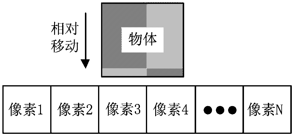
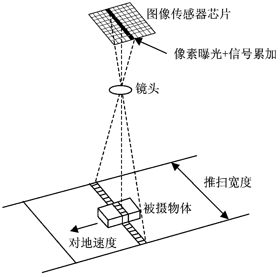
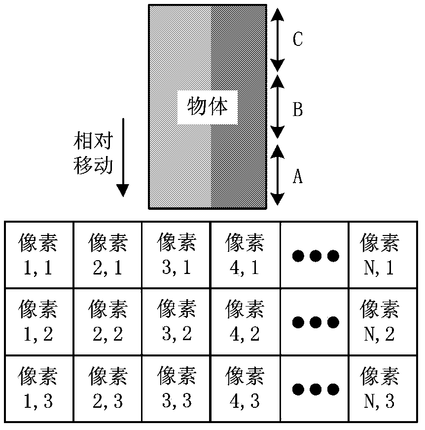
technical field [0001] The invention belongs to the technical field of TDI image sensors, and relates to a CMOS TDI image sensor and a charge transfer control method thereof. Background technique [0002] Time Delay Integration (TDI for short) is a sensor technology that can obtain high signal-to-noise ratio images when the imaging carrier or the measured object is moving rapidly. It is a line scan image sensor (such as figure 1 shown) is an evolution. The working principle of the line scan image sensor is that when the object moves relatively, the sensor performs continuous exposure, and transfers and stores the signal generated by each exposure, and stitches it into a two-dimensional image in the later stage. However, if the object moves at high speed, the corresponding exposure time of each pixel will be shortened, so that the number of photons received by each pixel will be reduced, resulting in a decrease in the signal-to-noise ratio (SNR) of the image and poor image q...

Claims


Application Information

Patent Timeline
Patent Type & Authority Applications(China)
IPC IPC(8): H04N5/359H04N5/374
Inventor 阿德里·米尔普李扬马成王欣洋
Owner GPIXEL
Why Eureka
Try Eureka