Three-dimensional electrode pattern manufacturing method

A technology of three-dimensional electrode and manufacturing method, which is applied in the field of micro-mechanical technology, can solve the problems of increasing difficulty of the process, and achieve the effect of simple process of process and high precision of graphic production

Active Publication Date: 2013-11-27
CHINA ELECTRONICS TECH GRP NO 26 RES INST
View PDF5 Cites 6 Cited by
  • Summary
  • Abstract
  • Description
  • Claims
  • Application Information

AI Technical Summary

Problems solved by technology

This method has high precision in making electrode patterns, but the photoresist before photolithography needs to be sprayed with special spraying glue equipment, which increases the difficulty of the process, and requires the purchase of spraying glue equipment before the process can be produced

Method used


Image

  • Three-dimensional electrode pattern manufacturing method
  • Three-dimensional electrode pattern manufacturing method
  • Three-dimensional electrode pattern manufacturing method

Examples


Embodiment approach 2

[0068] In the second embodiment, in the step of etching the patterned mask layer 2 to obtain a three-dimensional electrode pattern, the etching solution used for etching the patterned mask layer 2 cannot corrode the protective film metal layer 6 . In the step of removing the protective film metal layer 6 , the etching solution used to corrode the protective film metal layer 6 cannot corrode the patterned mask layer 2 .

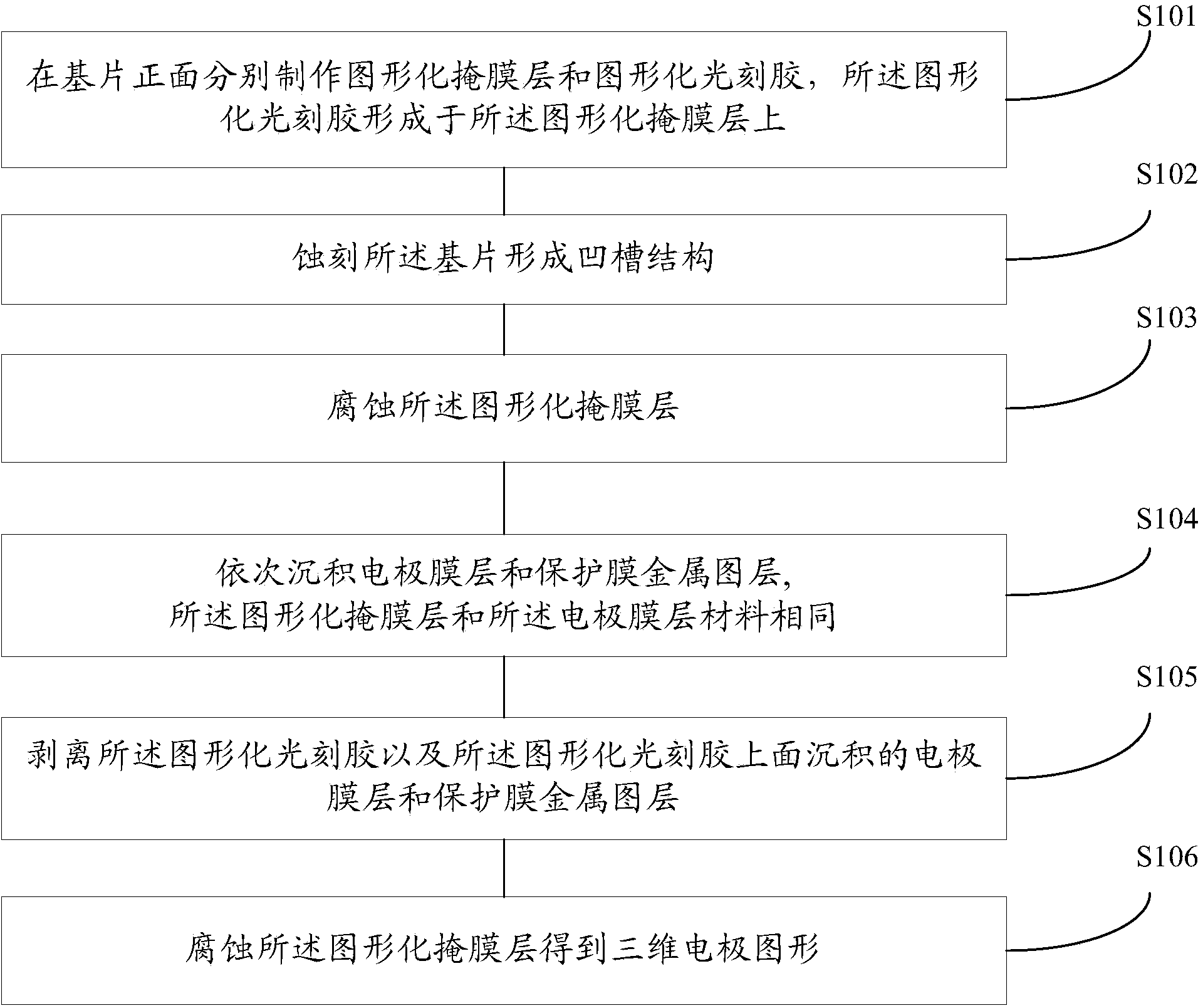
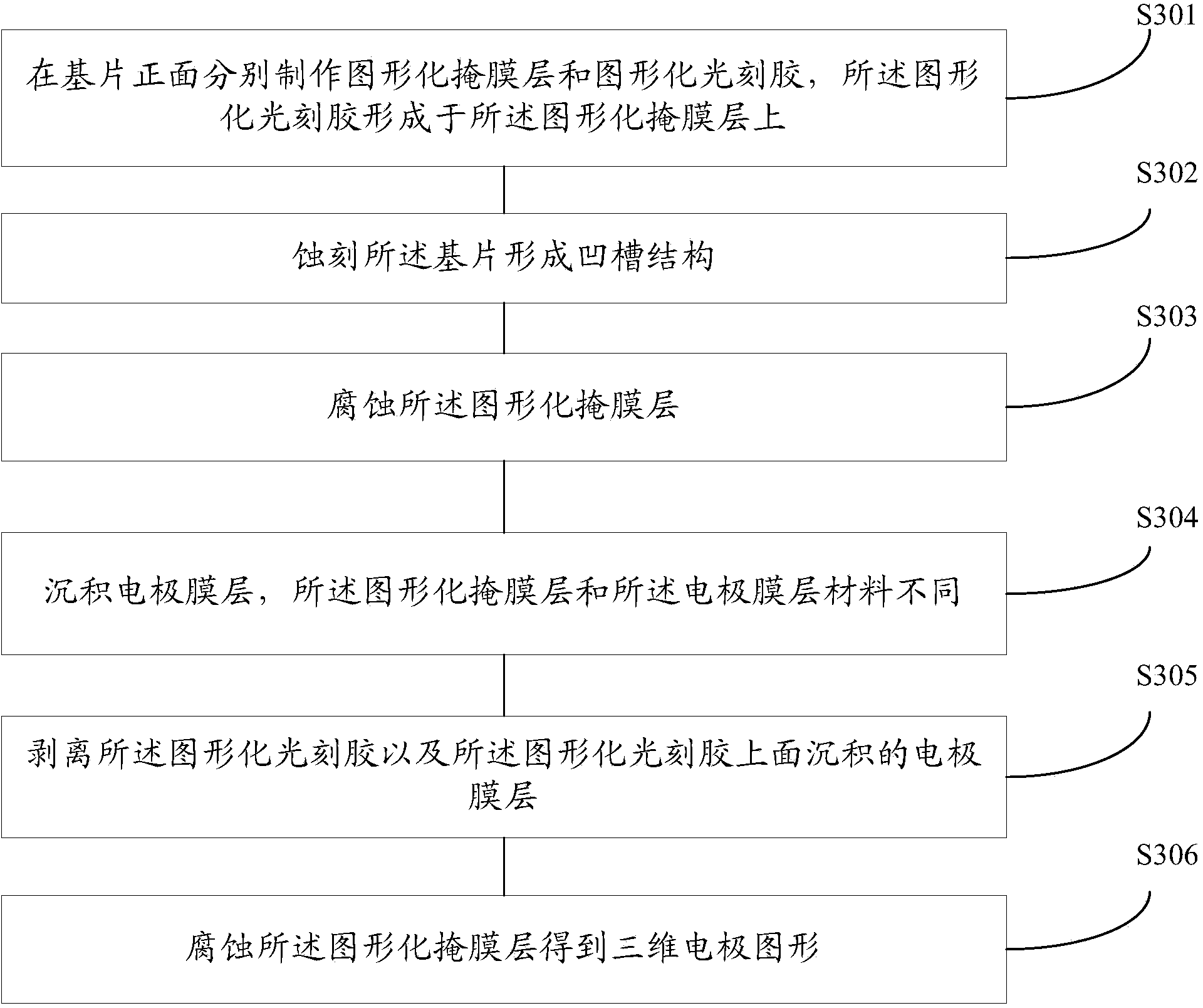
[0069] See image 3 , the three-dimensional electrode pattern manufacturing method of the third embodiment of the present invention, comprising the following steps:

[0070] S301, respectively fabricating a patterned mask layer and a patterned photoresist on the front surface of the substrate, the patterned photoresist being formed on the patterned mask layer;

[0071] S302, etching the substrate to form a groove structure;

[0072] S303, etching the patterned mask layer;

[0073] S304, depositing an electrode film layer, the material of the patterned mask ...

Embodiment approach 3

[0076] In the method of Embodiment 3, in S306, after the directly exposed patterned mask layer is etched away, the electrode film layer with a predetermined pattern is left to cover the substrate.

[0077] Compared with the method in Embodiment 1, in Embodiment 3, the materials of the patterned mask layer and the electrode film layer are different, and there is no need to deposit a protective film metal layer in step S304.

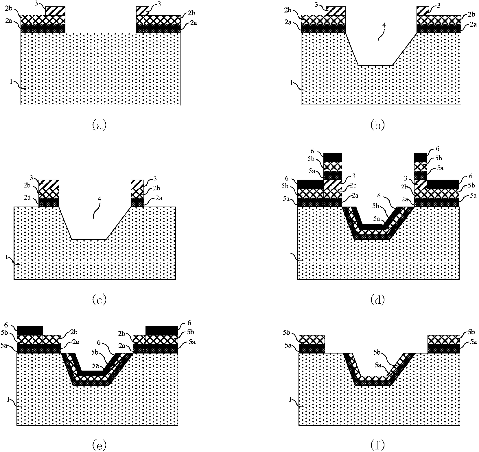
[0078] See Figure 4 (a) to (e), the principle of the three-dimensional electrode pattern manufacturing method in the fourth embodiment of the present invention is the same as that in the third embodiment.

[0079] Among them, such as Figure 4 As shown in (a), a patterned mask layer 11 and a patterned photoresist 12 are respectively formed on the front surface of the substrate 10 . Wherein, the patterned mask layer 11 includes a lower film layer 11a and an upper film layer 11b.

[0080] The steps of making a patterned mask layer 11 and a patterned phot...


PUM


Abstract

The invention provides a three-dimensional electrode pattern manufacturing method. The three-dimensional electrode pattern manufacturing method comprises the following steps: manufacturing a graphical mask layer and graphical photoresist respectively on the front face of a substrate, wherein the graphical photoresist is formed on the graphical mask layer; etching the substrate to form a groove structure; corroding the graphical mask layer; deposting an electrode film layer and a protective film metal layer in sequence, wherein the graphical mask layer and the electrode film layer are made of a same material; peeling off the graphical photoresist as well as the electrode film layer and the protective film metal layer deposited on the graphical photoresist; corroding the graphical mask layer to obtain a three-dimensional electrode pattern. According to the method, the manufacturing of the three-dimensional electrode pattern is realized by adopting a peeling-off technology, special adhesive spraying equipment is not required to be bought, the manufacturing process is simple, and the pattern manufacturing precision is high.

Description

technical field [0001] The invention relates to the technical field of micro-mechanical technology, in particular to a manufacturing method capable of realizing three-dimensional electrode graphics. Background technique [0002] The micro-mechanical (MEMS) process originated from the semiconductor process. The semiconductor process is a planar process, while the micro-mechanical process is a three-dimensional process. Various complex three-dimensional structures can be processed by using the micro-mechanical process. [0003] After the three-dimensional micro-mechanical structure is processed by the micro-mechanical (MEMS) process, some devices need to make electrode patterns on the front and side of the structure in order to extract the required electrical signals. [0004] By searching the non-patent literature, we found the literature "A Z-Axis Quartz Cross-Fork Micromachined Gyroscope Based on Shear Stress Detection" published by Liqiang Xie et al. on "Sensors2010". A m...

Claims


Application Information

Patent Timeline
Patent Type & Authority Applications(China)
IPC IPC(8): B81C1/00
Inventor 林丙涛
Owner CHINA ELECTRONICS TECH GRP NO 26 RES INST
Why Eureka
Try Eureka