Splicing exposing method for photo-etched large-size CCD (Charge Coupled Device) chip

An exposure method and a large-scale technology, which are applied in microlithography exposure equipment, photolithography exposure devices, optics, etc., can solve problems such as narrowing, widening of lines, and deformation of geometric connections, so as to improve performance or quality Effect

Active Publication Date: 2013-11-27
THE 44TH INST OF CHINA ELECTRONICS TECH GROUP CORP
View PDF6 Cites 24 Cited by
  • Summary
  • Abstract
  • Description
  • Claims
  • Application Information

AI Technical Summary

Problems solved by technology

[0004] In order to solve the problem that the geometric figures corresponding to the circuit structure of adjacent CCD splicing chips in the splicing exposure method of large-size CCD chips in lithography in the prio

Method used


Image

  • Splicing exposing method for photo-etched large-size CCD (Charge Coupled Device) chip
  • Splicing exposing method for photo-etched large-size CCD (Charge Coupled Device) chip
  • Splicing exposing method for photo-etched large-size CCD (Charge Coupled Device) chip

Examples


Embodiment Construction

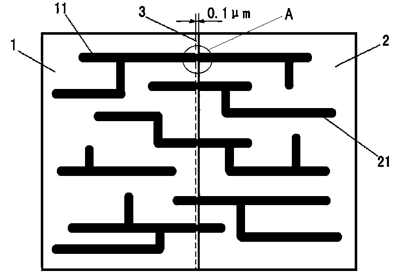
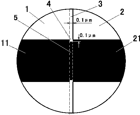
[0022] attached figure 1 It is a schematic diagram of making a large-size CCD chip by means of splicing photolithography exposure. In the figure, A, B, C and D are four CCD splicing chips of a large-size CCD chip. It can be seen from the figure that in practical applications, the size of a single CCD chip is larger than the maximum exposure field of view of a lithography machine. For example, the chip size of a long line array CCD is 2mm×80mm, and the size of a large area array CCD chip even reaches 96 mm×96mm . Although the wafer required to make a large-size CCD chip can meet its size requirements, due to the limitation of the maximum exposure field of view of the lithography machine, it is still impossible to transfer the geometry on the mask plate to the wafer through one exposure. It is processed by splicing exposure. The so-called splicing exposure refers to dividing a large-size CCD chip into several CCD splicing chips whose size is smaller than or equal to the maximu...


PUM


Abstract

The invention provides a splicing exposing method for a photo-etched large-size CCD (Charge Coupled Device) chip, which aims at overcoming defects such as deformation, incoherence, and circuit widening or narrowing at the joint of geometric figures corresponding to adjacent CCD splicing chip circuit structures in the splicing exposing method for the photo-etched large-size CCD chip in the prior art. According to the splicing exposing method for the photo-etched large-size CCD chip, each CCD splicing chip is independently exposed in a splicing manner. The splicing exposing method is characterized in that an overlay region which has the width of 0.1 micrometer and is overlapped with a next photo-mask plate is arranged at the splicing side of the figure of the last photo-mask plate, and furthermore, 0.1*0.1-micrometer square compensation gaps are formed in the end heads of the geometric figures in the overlay region. The splicing exposing method has the beneficial technical effects that the defects such as the deformation, the incoherence, and the circuit widening or narrowing at the joint of the geometric figures corresponding to the adjacent CCD splicing chip circuit structures can be effectively avoided, and the performance or the quality of the large-size CCD chip can be effectively improved.

Description

[0001] field of invention [0002] The invention relates to a large-size CCD chip preparation technology, in particular to a photoetching large-size CCD chip splicing exposure method. Background technique [0003] The exposure process is a very important process in the process of making CCD chips. Its purpose is to transfer the geometric figures on the photolithographic mask to the wafer, and then form a circuit structure on the wafer through etching and other processes, so as to produce a CCD chip with photoelectric function. Obviously, the geometry on the photolithographic mask is essentially the circuit structure of the CCD chip, which is transferred to the wafer by exposure. At present, the mainstream lithography machines used in the CCD chip lithography process are stepping lithography machines and scanning lithography machines. The maximum exposure fields of these two lithography machines are 22mm×22mm and 26mm×33mm respectively. In practical applications, the size o...

Claims


Application Information

Patent Timeline
IPC IPC(8): G03F7/20G03F7/00
Inventor 李佳刘方杨洪高建威邓涛
Owner THE 44TH INST OF CHINA ELECTRONICS TECH GROUP CORP
Why Eureka
Try Eureka