Supercharge Your Innovation With Domain-Expert AI Agents!

High power consumption chip packaging structure

A chip packaging structure, high power consumption technology, applied in electrical components, electrical solid devices, circuits, etc., can solve the problems of poor heat dissipation of high-power chips, increased packaging costs, etc., to improve system signal integrity and power integrity, The effect of reducing junction temperature difference and low process complexity

Active Publication Date: 2013-11-27
POWERTECH TECH SUZHOU
View PDF3 Cites 3 Cited by
  • Summary
  • Abstract
  • Description
  • Claims
  • Application Information

AI Technical Summary

Problems solved by technology

[0003] The purpose of the present invention is to provide a great merit that can solve the problem of poor heat dissipation of high-power chips in the traditional plastic package bonded package structure without changing the package form or adding additional heat sinks to replace the package structure, resulting in an increase in package cost. consumption chip package structure

Method used


Image

  • High power consumption chip packaging structure

Examples


Embodiment

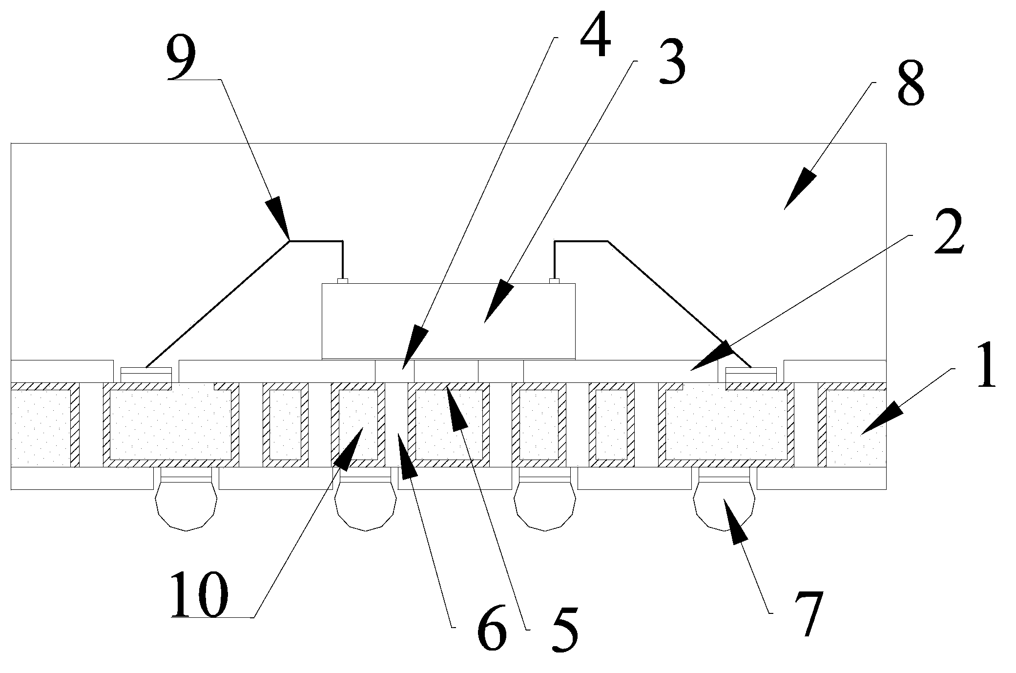
[0025] Such as figure 1 Shown: a large power consumption chip packaging structure, including: a substrate 1, with a top surface and a bottom surface opposite; the inside of the substrate 1 is a substrate 10, and the surface of the substrate 1 is an etched metal circuit layer 5, The metal circuit layer 5 is also coated with a solder resist layer 2;

[0026] It also includes a chip 3, which is arranged on the top surface of the substrate 1; directly below the chip 3 and on the solder resist layer 2 of the substrate 1, a plurality of green oil openings 4 are arranged, and the areas of the green oil openings 4 are exposed The metal circuit layer 5 is directly in contact with the chip 3;

[0027] It also includes a plurality of via holes 6 arranged on the substrate 1 and arranged under the chip 3;

[0028] It also includes a plurality of heat dissipation solder balls 7, which are arranged on the bottom surface of the substrate 1, and the heat dissipation solder balls 7 are welded...


PUM


Abstract

The invention discloses a high power consumption chip packaging structure, which is characterized by comprising a substrate, a chip, a plurality of through holes, a plurality of radiating solder balls and insulating resin, wherein the substrate is provided with a top surface and a bottom surface which are opposite to each other; the internal part of the substrate is a base material, the surface of the substrate is an etched metal line layer, and the metal line layer is coated with a solder resisting layer; the chip is configured on the top surface fo the substrate; a plurality of green oil windows are arranged in the solder resisting layer of the substrate just below the chip, and the exposed metal line layer in the green oil window regions is in direct contact with the chip; the plurality of through holes are arranged in the substrate below the chip; the plurality of solder balls are configured on the bottom surface of the substrate and are welded on a PCB board; and the insulating resin is filled in a packaging space of the packaging structure. The high power consumption chip packaging structure has the advantages of low technical complexity and considerable cost comparative advantage, has better radiating effect for the high power consumption packaged chips when compared with existing main mainstream bonding plastic packaging technology, and can significantly reduce the temperature difference of the chip surface junction temperature.

Description

technical field [0001] The invention belongs to the technical field of semiconductor memory packaging, and in particular relates to a large power consumption chip packaging structure, which effectively solves the heat dissipation problem of the high power consumption chip in the bonded BGA package. Background technique [0002] The power consumption of traditional chips generally does not exceed 0.5W, while the power consumption of high-power chips used in bonding BGA packaging structures is 2-5W. Since the power consumption is 4-10 times higher than that of traditional chips, the corresponding heat dissipation problem is also It is highlighted that the traditional bonded plastic package structure can no longer satisfy the heat dissipation of high-power consumption chips. During use, due to the large heat generation, poor heat dissipation is prone to occur, which will lead to increased damage rates of components and poor reliability. Some existing technical improvements can ...

Claims


Application Information

Patent Timeline
Patent Type & Authority Applications(China)
IPC IPC(8): H01L23/498
CPCH01L2224/48227H01L2924/15311
Inventor 陆春荣胡立栋金若虚刘鹏
Owner POWERTECH TECH SUZHOU
Features
  • R&D
  • Intellectual Property
  • Life Sciences
  • Materials
  • Tech Scout
  • Unparalleled Data Quality
  • Higher Quality Content
  • 60% Fewer Hallucinations
Learn More