
Broadband full-sealed package of microwave devices

A microwave device, fully sealed technology, applied in the direction of electric solid-state devices, semiconductor devices, semiconductor/solid-state device parts, etc., can solve the problems of reducing thermal impedance, high thermal impedance, and fully-sealed packaging cannot work, etc., to achieve good impedance Matching, reducing the effect of coupling

Active Publication Date: 2013-12-04
GUANGZHOU STARWAY COMM TECH
View PDF3 Cites 9 Cited by
  • Summary
  • Abstract
  • Description
  • Claims
  • Application Information

AI Technical Summary

Problems solved by technology

The fully-sealed package needs to use a metal sealing strip. When the signal frequency is higher than 20GHz, it will cause the metal strip to resonate. Therefore, the fully-sealed package usually cannot work in a wide frequency band such as DC to 20GHz and above.
[0003] Most microwave device packages use ceramic itself or filled vias for heat conduction. This heat sink has high thermal impedance and poor thermal conductivity, and is not suitable for high-power amplifiers that generate high heat.
The package of a high power amplifier generally uses a large metal base to reduce thermal impedance, but this package is not surface mounted, but fixed on the shell with screws. Such a package is not only bulky, but the installation process is also very complicated. None of the

Method used


Image

  • Broadband full-sealed package of microwave devices
  • Broadband full-sealed package of microwave devices
  • Broadband full-sealed package of microwave devices

Examples


Embodiment Construction

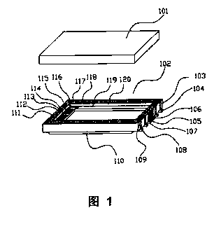
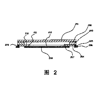
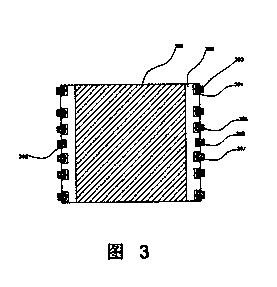
[0022] figure 1 For package perspective view. The entire package includes a cover 101 and a package body 102 . The package body 102 includes a ceramic frame 103 , a metal base 110 and a plurality of metal pins 104 .

[0023] The ceramic frame 103 is composed of multilayer ceramics. It can be made of high temperature co-fired ceramic (HTCC) or low temperature co-fired ceramic (LTCC) process, the HTCC process is more robust. In the production process, when the ceramics are still in the state of cement, the metal wires are printed on each layer of the substrate, and via holes are made to fill the metal material in the state of cement. Then put the first layer (lower layer) ceramics 119 and the second layer (upper layer) ceramics 120 together into the furnace for firing. These two layers of ceramics will become an integrated ceramic frame 103 . The metal base 110 and the metal pins 104 are respectively welded to the ground plane and the pad on the bottom surface of the cerami...


PUM


Abstract

The invention discloses a ceramic full-sealed surface package of microwave devices. A ceramic frame of the package is arranged on a substrate, wherein the substrate can serve as a circuit which is grounded and also have the heat dissipation function. The cavity in the ceramic frame is used for containing MMICs or other microwave devices. The substrate is slightly smaller than the ceramic frame so that metal pins can be welded to the bottom of the ceramic frame, and the metal pins and the substrate are located in the same plane. Radio-frequency and direct current conductive wires on the first layer of ceramic of the package are connected with devices inside the package and connected to the outside of the package through via holes. The package can also not be provided with the pins additionally, and bonding pads of the ceramic frame are directly welded to a printed circuit board. A layer of metal sealing ring is deposited on the upper side of the second layer of ceramic to achieve full sealing. The sealing ring is grounded through a conductive via hole penetrating through the ceramic. The full-sealed package can eliminate resonance in a very wide frequency band and reduce the parasitic effect to the minimum, thereby achieving good broadband performance. Meanwhile, the package has the excellent heat dissipation function and therefore can be widely applied to a great number of high-power devices.

Description

Technical field [0001] The patent of the present invention relates to a fully sealed microwave device surface package using ceramic materials. Background technique [0002] Most existing microwave device packages are sealed with epoxy resin instead of fully sealed packages. The fully-sealed package needs to use a metal sealing strip. When the signal frequency is higher than 20GHz, the metal strip will resonate. Therefore, the fully-sealed package usually cannot work in a wide frequency band such as DC to 20GHz and above. [0003] Most microwave device packages use ceramic itself or filled vias for heat conduction. This heat sink has high thermal impedance and poor thermal conductivity, and is not suitable for high-power amplifiers that generate high heat. The package of a high power amplifier generally uses a large metal base to reduce thermal impedance, but this package is not surface mounted, but fixed on the shell with screws. Such a package is not only bulky, but the in...

Claims


Application Information

Patent Timeline
IPC IPC(8): H01L23/48H01L23/66
CPCH01L2924/0002H01L2924/00
Inventor 贾鹏程
Owner GUANGZHOU STARWAY COMM TECH
Learn More