Wafer level camera shooting module WLC automatic testing socket

A camera module and automatic testing technology, which is applied in the direction of single semiconductor device testing, measuring device casing, etc., can solve the problems of easy open circuit and short circuit, reliability problem, complex structure, etc., and achieve prolonging service life, convenient use and easy operation simple effect

Inactive Publication Date: 2013-12-11
SUZHOU CHUANGRUI MACHINERY & ELECTRICAL TECH
View PDF6 Cites 4 Cited by
  • Summary
  • Abstract
  • Description
  • Claims
  • Application Information

AI Technical Summary

Problems solved by technology

[0003] At present, most of the CMOS imaging modules are loaded with flexible circuit boards for SMT assembly, and the structure is relatively complicated. Due to the large number of components, the functions realized are not as direct and reliable as WLC imaging modules.
Correspondingly, the existing module test socket is suitable for the structure of the existing camera module. For functional testing, ICT probes are generally used for detection. The structure is complex and prone to open and

Method used


Image

  • Wafer level camera shooting module WLC automatic testing socket
  • Wafer level camera shooting module WLC automatic testing socket
  • Wafer level camera shooting module WLC automatic testing socket

Examples


Embodiment Construction

[0025] The technical solution of the present invention will be further described below in conjunction with the accompanying drawings and a preferred embodiment.

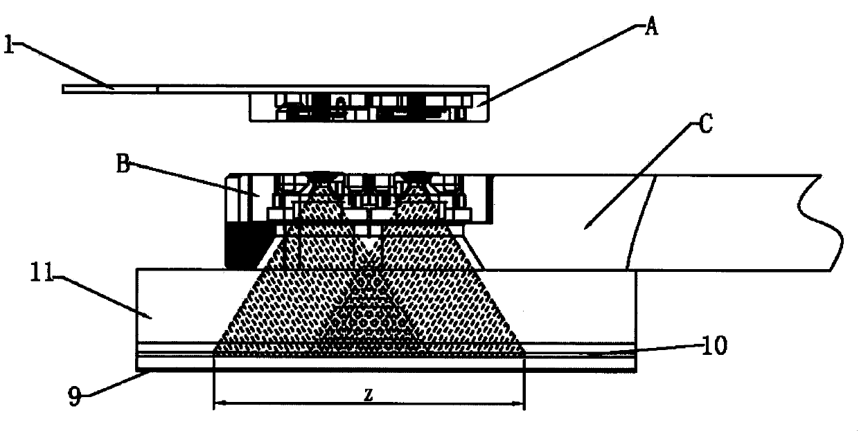
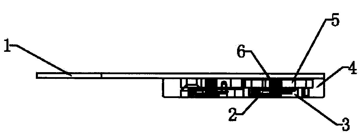
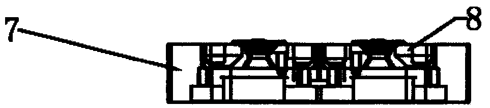
[0026] refer to figure 1 , a wafer-level camera module WLC automatic test socket A involved in this embodiment includes a base, a module placement structure B and a light source unit, and the base is connected to a PCB adapter board 1, wherein the base includes The test unit installed in the socket holding frame 4, the test unit includes a plurality of test probes 6 and the probe holding main body 2 and the probe holding plate 5 distributed in sequence along the direction away from the PCB adapter board, the module The placement structure includes a placement and retention frame 7 and a floating plate 3, the placement and retention frame is provided with at least one module placement groove 8, the floating plate is arranged between the module placement groove and the probe holding main body, the light source unit In...


PUM


Abstract

The invention discloses a wafer level camera shooting module WLC automatic testing socket which comprises a base, a module placing structure and a light source unit. The base is connected with a PCB pinboard. The base comprises a test unit which is mounted in a socket maintaining frame. The test unit comprises a plurality of test probes, a probe maintaining main body and a probe maintaining plate, wherein the probe maintaining main body and the probe maintaining plate are sequentially distributed in the direction far away from the PCB pinboard. The module placing structure comprises a placing maintaining frame and a floating plate, the placing maintaining frame is provided with at least one module placing groove, and the floating plate is arranged between the module placing groove and the probe maintaining main body. The light source unit comprises an LED lamp panel and a standard plate which are arranged inside a camera obscura. The module placing groove, a lens connected to the placing maintaining frame, the LED lamp panel and the standard plate are sequentially distributed in the direction far away from the PCB pinboard. The wafer level camera shooting module WLC automatic testing socket can be compatible with different testing machines, automatic, efficient and accurate testing of a WLC module can be achieved, and the module and a chip can not be damaged.

Description

technical field [0001] The invention relates to a chip testing device, in particular to a wafer-level camera module WLC automatic testing socket. Background technique [0002] Wafer-level camera module WLC series is a new type of CMOS chip imaging integrated system developed by American APTINAIMAGING and Kunshan Xitai QTECH. Wafer Level Optical Lens WLO (Wafer Level Optical) WLO is assembled to form a camera pair module. [0003] At present, most of the CMOS imaging modules are loaded with flexible circuit boards for SMT assembly, and the structure is relatively complicated. Due to the large number of components, the functions realized are not as direct and reliable as WLC imaging modules. Correspondingly, the existing module test socket is suitable for the structure of the existing camera module. For functional testing, ICT probes are generally used for detection. The structure is complex and prone to open and short circuits; the stability is poor. The service life is gre...

Claims


Application Information

Patent Timeline
IPC IPC(8): G01R1/04G01R31/26
Inventor 朱小刚柳慧敏
Owner SUZHOU CHUANGRUI MACHINERY & ELECTRICAL TECH
Why Eureka
Try Eureka