Copper foil for printed circuit

A printed circuit, copper foil technology, applied in the direction of printed circuit, printed circuit, printed circuit manufacturing, etc.

Active Publication Date: 2013-12-11
JX NIPPON MINING & METALS CORP
View PDF11 Cites 6 Cited by
  • Summary
  • Abstract
  • Description
  • Claims
  • Application Information

AI Technical Summary

Problems solved by technology

[0016] Although this technology is effective, Ni may be contained not only in the zinc-nickel alloy layer, but also in all layers of the roughening treatment layer, heat-resistant layer, and weather-resistant layer. Copper foil for printed circuits with very good corrosion and general FPC characteristics requires further research on the total Ni content of all layers of the roughening treatment layer, heat-resistant layer, and weather-resistant layer

Method used


Image

  • Copper foil for printed circuit
  • Copper foil for printed circuit
  • Copper foil for printed circuit

Examples


Embodiment 1

[0134] (Conditions of Example 1)

[0135] The heat-resistant layer including the Ni—Co layer, the weather-resistant layer and the rust-proof layer including Zn, Ni, and Cr, and the silane coupling treatment were performed within the range of the conditions shown above. Conditions for forming a heat-resistant layer, a weather-resistant layer, and a rust-resistant layer are as follows.

[0136] 1) Heat-resistant layer (Ni-Co layer)

[0137] Current density (D k ): 5~15A / dm 2

[0138] Time: 0.05~3.0 seconds

[0139] 2) Weather-resistant layer (Zn-Ni layer)

[0140] Current density (D k ): 0.5~1.5A / dm 2

[0141] Time: 0.05~3.0 seconds

[0142] 3) Antirust layer (Cr-Zn layer)

[0143] Current density (D k ): 1~3A / dm 2

[0144] Time: 0.05~3.0 seconds

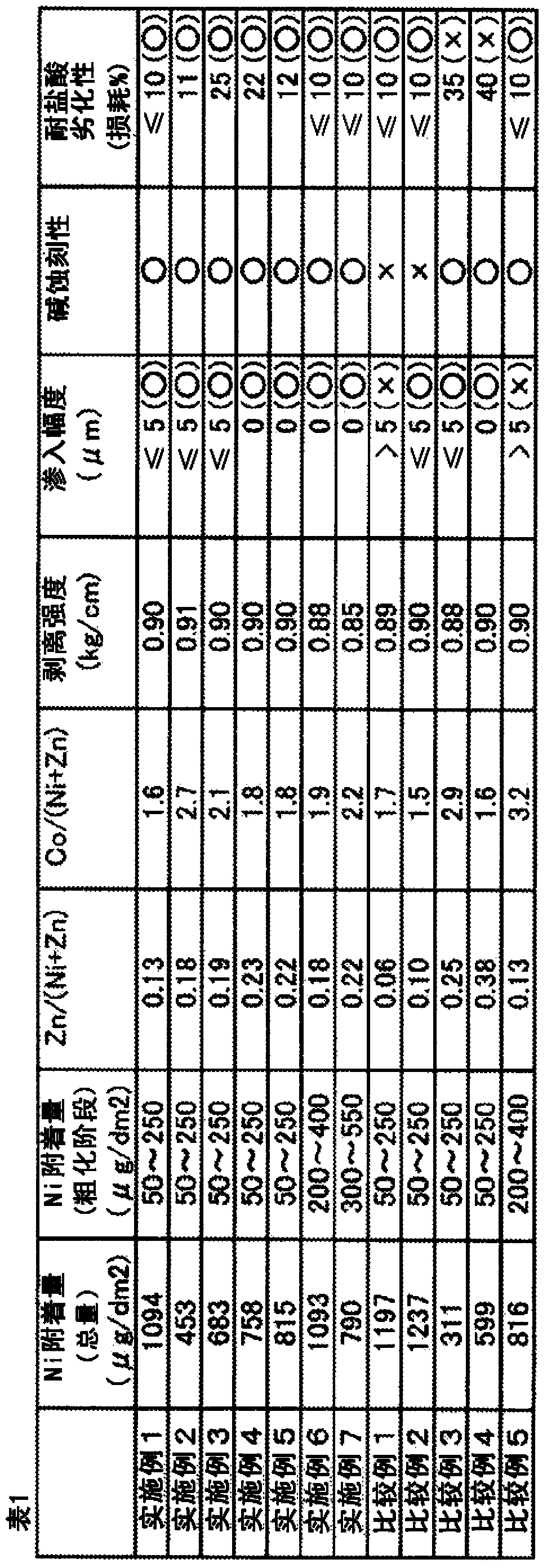
[0145] In order to make the Ni adhesion amount in all layers of roughening treatment layer, heat-resistant layer and weather-resistant layer be 1094μg / dm in total 2 The way to implement plating treatment. Zn / (Ni+Zn)=0....

Embodiment 2

[0158] As mentioned above, the amount of Ni deposited in the roughening stage is 50-250μg / dm 2 .

[0159] The heat-resistant layer including the Ni—Co layer, the weather-resistant layer and the rust-proof layer including Zn, Ni, and Cr, and the silane coupling treatment were performed within the range of the conditions shown above. Conditions for forming a heat-resistant layer, a weather-resistant layer, and a rust-resistant layer are as follows.

[0160] 1) Heat-resistant layer (Ni-Co layer)

[0161]Current density (D k ): 5~9A / dm 2

[0162] Time: 0.05~3.0 seconds

[0163] 2) Weather-resistant layer (Zn-Ni layer)

[0164] Current density (D k ): 0.05~0.7A / dm 2

[0165] Time: 0.05~3.0 seconds

[0166] 3) Antirust layer (Cr-Zn layer)

[0167] Current density (D k ): 1~3A / dm 2

[0168] Time: 0.05~3.0 seconds

[0169] The total amount of Ni attached to all layers of the roughening treatment layer, heat-resistant layer, and weather-resistant layer is 453 μg / dm 2 , ...

Embodiment 3

[0173] As mentioned above, the amount of Ni deposited in the roughening stage is 50-250μg / dm 2 .

[0174] The heat-resistant layer including the Ni—Co layer, the weather-resistant layer and the rust-proof layer including Zn, Ni, and Cr, and the silane coupling treatment were performed within the range of the conditions shown above. Conditions for forming a heat-resistant layer, a weather-resistant layer, and a rust-resistant layer are as follows.

[0175] 1) Heat-resistant layer (Ni-Co layer)

[0176] Current density (D k ): 6~11A / dm 2

[0177] Time: 0.05~3.0 seconds

[0178] 2) Weather-resistant layer (Zn-Ni layer)

[0179] Current density (D k ): 0.05~0.7A / dm 2

[0180] Time: 0.05~3.0 seconds

[0181] 3) Antirust layer (Cr-Zn layer)

[0182] Current density (D k ): 2~4A / dm 2

[0183] Time: 0.05~3.0 seconds

[0184] The total amount of Ni attached to all layers of the roughening treatment layer, heat-resistant layer, and weather-resistant layer is 683 μg / dm 2 ...


PUM

PropertyMeasurementUnit
particle sizeaaaaaaaaaa

Abstract

Provided is a copper foil with surface treatment layers, which is characterized by comprising a copper foil or copper alloy foil and, formed thereon, a plurality of surface treatment layers that comprise a roughened layer formed through a roughening treatment, a heat-resistant layer constituted of a Ni-Co layer formed on the roughened layer, and a weatherable layer and a rust-preventive layer which contain Zn, Ni, or Cr and have been formed on the heat-resistant layer, the surface treatment layers having a (total Zn) / [(total Zn)+(total Ni)] ratio of 0.13-0.23. Also provided is a copper foil for printed circuits which is obtained by forming a layer on a surface of a copper foil through a roughening treatment, subsequently forming a heat-resistant layer and a rust-preventive layer thereon, and then subjecting the rust-preventive layer to a treatment with a silane coupling agent. When a fine-pattern printed circuit is formed in a copper-clad laminate formed using the copper foil for printed circuits and the substrate thereafter is subjected to an acid treatment or chemical etching, then the decrease in adhesion due to acid infiltration into the interface between the copper foil circuit and the substrate resin can be more inhibited. Thus, the copper foil for printed circuits has excellent adhesion strength with respect to acid resistance and has excellent alkali etchability.

Description

technical field [0001] The present invention relates to a copper foil for a printed circuit and a copper-clad laminate, and in particular to a copper foil for a printed circuit. layer, anti-rust layer, and then silane coupling treatment. After forming a fine pattern printed circuit on the copper clad laminate using the copper foil for printed circuit, when acid treatment or chemical etching is performed on the substrate, it can be further suppressed. Copper foil for printed circuits with excellent acid-resistant adhesive strength and excellent alkali etching properties due to the decrease in adhesion caused by acid penetration into the interface between the copper foil circuit and the substrate resin. [0002] The copper foil for printed circuits of the present invention is suitable for, for example, flexible printed wiring boards (Flexible Printed Circuit, hereafter referred to as FPC) and fine pattern printed circuits. Background technique [0003] Copper and copper alloy...

Claims


Application Information

Patent Timeline
Patent Type & Authority Applications(China)
IPC IPC(8): C25D7/06C25D5/10H05K1/09
CPCC25D7/0614H05K3/388H05K3/389H05K2201/0352C25D5/14C25D5/48H05K3/384H05K2201/0355H05K2203/0723Y10T428/12076Y10T428/12438Y10T428/12049H05K1/09C25D5/605
Inventor 新井英太三木敦史
Owner JX NIPPON MINING & METALS CORP
Why Eureka
Try Eureka