Method for isolating device

A device isolation and wafer technology, applied in semiconductor/solid-state device manufacturing, electrical components, circuits, etc., can solve the problems of plasma damage, device performance degradation, high process difficulty, etc., to achieve the effect of ensuring isolation and reducing plasma damage

Active Publication Date: 2014-01-01
WUHAN XINXIN SEMICON MFG CO LTD
View PDF3 Cites 7 Cited by
  • Summary
  • Abstract
  • Description
  • Claims
  • Application Information

AI Technical Summary

Problems solved by technology

The existing isolation technologies include LOCOS and STI, but due to the increasingly high requirements for device isolation, a new technology of deep trench filling (DTI, deep trench isolation) is gradually being formed. Because deep trenches need to be etched, the process is more difficult High, and will cause device performance degradation due to more plasma damage

Method used


Image

  • Method for isolating device
  • Method for isolating device

Examples


Embodiment Construction

[0020] The principles and features of the present invention are described below in conjunction with the accompanying drawings, and the examples given are only used to explain the present invention, and are not intended to limit the scope of the present invention.

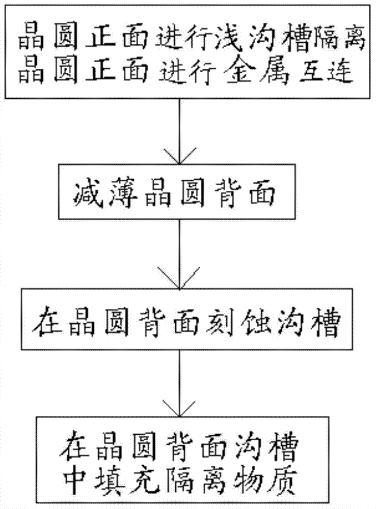
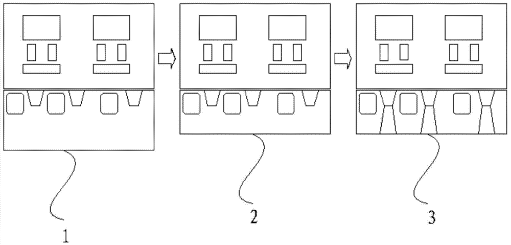
[0021] Such as figure 1 As shown, a device isolation method, first of all, shallow trench isolation is performed on the front of the wafer, and metal interconnection is performed on the front of the wafer. The shallow trench isolation is below 0.25um. trenches, filled trenches, and chemical-mechanical polishing and planarization technologies to isolate devices. The metal interconnection refers to depositing metal films on integrated circuits and forming wiring through photolithography techniques, and separating the mutually isolated components according to certain requirements. Interconnected into the desired circuit, the shallow trench etched on the front side of the wafer is located between the two doped regions o...


PUM


Abstract

The invention relates to a method for isolating a device. The method for isolating the device comprises the following steps that firstly, shallow trench isolation is conducted between two doping zones on the front face of a wafer and metal interconnection is conducted on the front face of the wafer; secondly, the back face of the wafer with metal interconnected is thinned; thirdly, trenches are etched on the back face of the wafer after the back face is thinned; fourthly, the trenches etched on the back face of the wafer are filled with isolating substances. Trenches are etched on the back face of a silicon substrate so that plasma damage caused by the operation that deep trenches are etched on the front face of the wafer can be reduced and meanwhile the isolating effect on the device can be guaranteed.

Description

technical field [0001] The invention relates to a device isolation method. Background technique [0002] Complementary metal oxide semiconductor (CMOS) is composed of P-type metal oxide semiconductor (PMOS) and N-type metal oxide semiconductor (NMOS). Because PMOS and NMOS need to be formed on the same silicon substrate at the same time, it is necessary to Quarantine. The existing isolation technologies include LOCOS and STI, but due to the increasingly high requirements for device isolation, a new technology of deep trench filling (DTI, deep trench isolation) is gradually being formed. Because deep trenches need to be etched, the process is more difficult High, and will cause device performance degradation due to more plasma damage. Contents of the invention [0003] The technical problem to be solved by the invention is to provide a simple device isolation method that reduces plasma damage and improves device performance. [0004] The technical solution of the present...

Claims


Application Information

Patent Timeline
Patent Type & Authority Applications(China)
IPC IPC(8): H01L21/762
CPCH01L21/02016H01L21/76224
Inventor 洪齐元黄海
Owner WUHAN XINXIN SEMICON MFG CO LTD
Why Eureka
Try Eureka