Array substrate, preparing method of array substrate and display device of array substrate

An array substrate and area technology, applied in semiconductor/solid-state device manufacturing, optics, instruments, etc., can solve problems such as unstable performance of thin film transistors and increased process difficulty

Active Publication Date: 2014-01-01
BOE TECH GRP CO LTD
View PDF6 Cites 12 Cited by
  • Summary
  • Abstract
  • Description
  • Claims
  • Application Information

AI Technical Summary

Problems solved by technology

[0003] When preparing the array substrate in the prior art, in order to reduce the number of patterning processes, a half-tone masking process is introduced to form the semiconductor active l

Method used


Image

  • Array substrate, preparing method of array substrate and display device of array substrate
  • Array substrate, preparing method of array substrate and display device of array substrate
  • Array substrate, preparing method of array substrate and display device of array substrate

Examples


Embodiment Construction

[0053] The following will clearly and completely describe the technical solutions in the embodiments of the present invention with reference to the accompanying drawings in the embodiments of the present invention. Obviously, the described embodiments are only some, not all, embodiments of the present invention. Based on the embodiments of the present invention, all other embodiments obtained by persons of ordinary skill in the art without making creative efforts belong to the protection scope of the present invention.

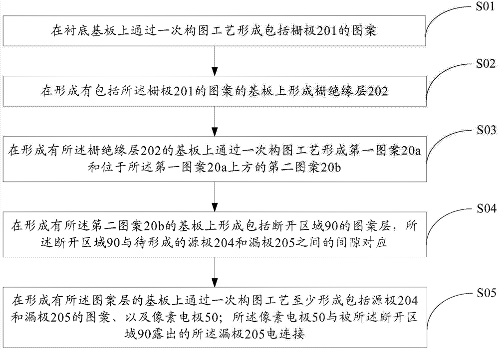
[0054] An embodiment of the present invention provides a method for preparing an array substrate 10, such as figure 1 As shown, the following steps may be included:

[0055] S01 , forming a pattern including a gate 201 on a base substrate through a patterning process.

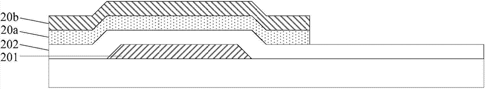
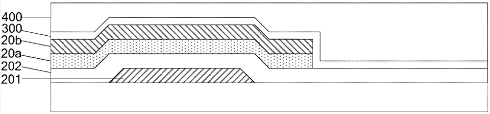
[0056] S02 , forming a gate insulating layer 202 on the substrate on which the pattern including the gate 201 is formed.

[0057] S03, forming a first pattern 20a and a second pattern 20b abo...


PUM


Abstract

An embodiment of the invention provides an array substrate, a preparing method of the array substrate and a display device of the array substrate and relates to the technical field of displaying. The use of halftone masking process is avoided, the process difficulty is simplified, and the cost is saved. The preparing method comprises the steps of using once composite picture process to form a pattern comprising a grid, forming a grid insulating layer on a substrate where the pattern comprising the grid is formed, using the once composite picture process to form a first pattern and a second pattern above the first pattern, forming a pattern layer comprising a broken area on a substrate where the second pattern is formed, and using the once composite picture process to at least form a pattern comprising a source electrode, a drain electrode and a pixel electrode which is electrically connected with the drain electrode through the broken area. In addition, the first pattern corresponds to a pattern of a semiconductor active layer, the second pattern corresponds to the source electrode and the drain electrode, the broken area corresponds to a gap between the source electrode and the drain electrode, the minimum width of the broken area is larger than that of the gap between the source electrode and the drain electrode, and at least the drain electrode is exposed out of the broken area. The array substrate is applied to manufacturing display devices.

Description

technical field [0001] The present invention relates to the field of display technology, in particular to an array substrate, a preparation method thereof, and a display device. Background technique [0002] Thin Film Transistor Liquid Crystal Display (TFT-LCD) has the characteristics of small size, low power consumption, and no radiation. It occupies a dominant position in the field of flat panel display technology and has attracted widespread attention. [0003] When preparing the array substrate in the prior art, in order to reduce the number of patterning processes, a half-tone masking process is introduced to form the semiconductor active layer and the source and drain electrodes through one patterning process, but this will increase the difficulty of the process, which may cause The instability of thin film transistor performance. [0004] In addition, in order to optimize the performance of the array substrate and increase its flatness, at least one pattern layer wit...

Claims


Application Information

Patent Timeline
IPC IPC(8): H01L27/12H01L21/84H01L23/50G02F1/1362G02F1/1368
CPCH01L27/124H01L27/1244H01L27/1248H01L27/1259H01L27/1288H01L29/66765H01L29/66969H01L29/78669H01L29/7869H01L29/78696
Inventor 孙双
Owner BOE TECH GRP CO LTD
Why Eureka
Try Eureka