Nonvolatile three-dimensional semiconductor memory device and preparing method

A non-volatile memory technology, applied in the direction of static memory, digital memory information, information storage, etc., can solve problems such as optimization, unfavorable storage performance, limitations, etc., to improve erasing speed, simplify process difficulty, and simplify process Effect

Active Publication Date: 2013-06-05
INST OF MICROELECTRONICS CHINESE ACAD OF SCI
View PDF3 Cites 9 Cited by
  • Summary
  • Abstract
  • Description
  • Claims
  • Application Information

AI Technical Summary

Problems solved by technology

Although the adoption of this gate-first process is simple, it substantially limits the selection of gate stack materials and gate electrode materials, which is not conducive to the optimization of storage performance.

Method used


Image

  • Nonvolatile three-dimensional semiconductor memory device and preparing method
  • Nonvolatile three-dimensional semiconductor memory device and preparing method
  • Nonvolatile three-dimensional semiconductor memory device and preparing method

Examples


Embodiment Construction

[0031] In order to make the object, technical solution and advantages of the present invention clearer, the present invention will be described in further detail below in conjunction with specific embodiments and with reference to the accompanying drawings.

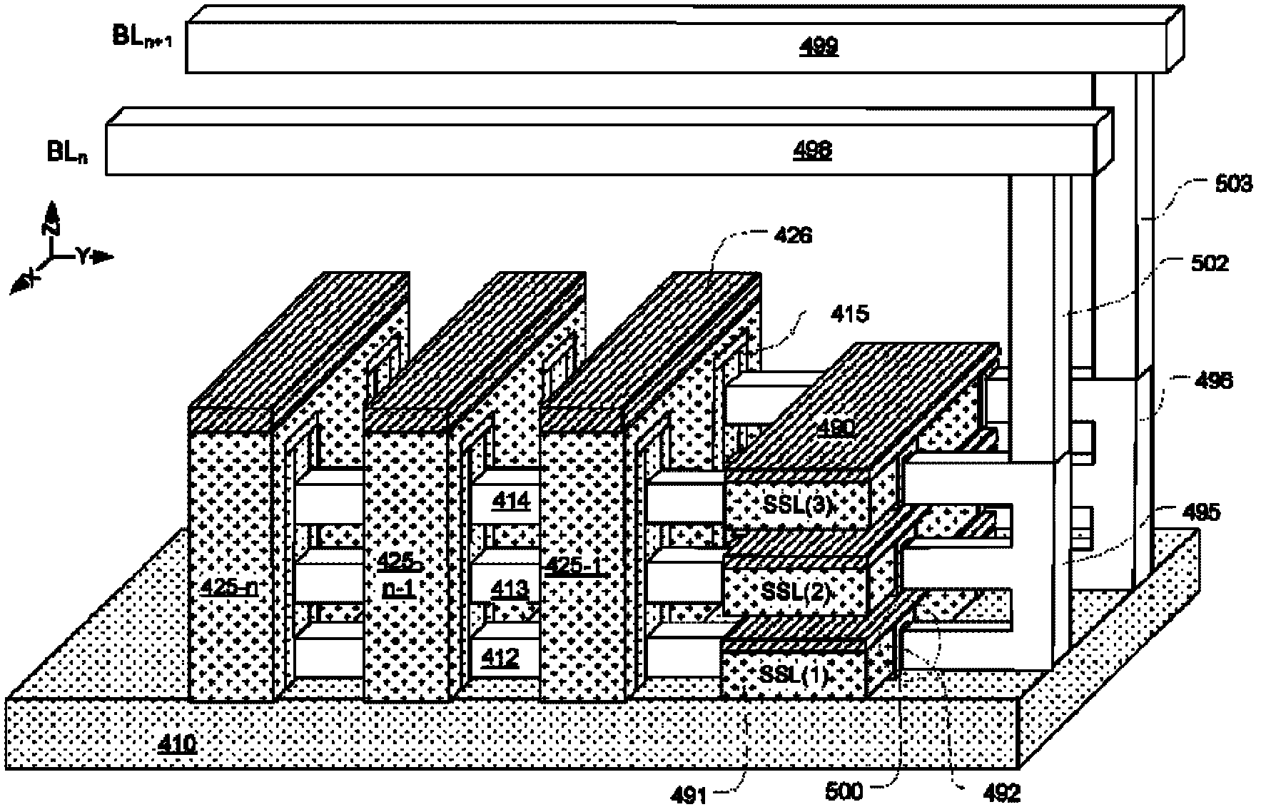
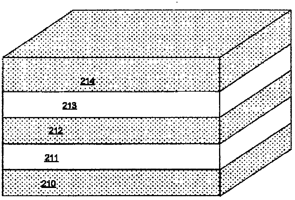
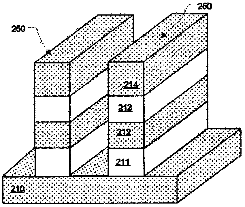
[0032] The preparation method of the non-volatile three-dimensional semiconductor memory provided by the present invention adopts the gate-last process instead of the gate-front process, and completes the isolation of the insulating layer outside the gate electrode region before the gate electrode is deposited, specifically including: forming an insulating layer on the substrate Alternate deposition with the conduction layer to form a stacked structure; use photolithography to etch the formed stacked structure to form multiple stacked strip-shaped conduction structures, and complete the etching isolation in the direction of the bit line; A resistive switch material or a phase change material is deposited on a substrate wit...


PUM


Abstract

The invention relates to the technical field of microelectronics, and discloses a nonvolatile three-dimensional semiconductor memory device and a preparing method. The three-dimensional semiconductor memory device comprises bit lines made of strip-shaped connecting materials which are isolated by a plurality of insulating layers; each strip-shaped connecting bit line is provided with two surface zones along the side direction; word lines made of connecting materials are arranged in the direction orthogonal with the connecting bit lines; and storage materials are placed in the middle of a cross-shaped overlapping zone which is then used as an electric charge capturing stack zone or a resistance changing function zone. High-dielectric-constant materials can be used in a function zone of the three-dimensional semiconductor memory device, and high-work function materials such as metal nitride are used in a gate electrode. Therefore, according to the preparing method of the three-dimensional semiconductor memory device, partitioning zones arranged between the word lines are introduced first, then storage function layer materials and gate materials are deposited in a back-gate technology, a technology is simplified, material pollution is avoided, and meanwhile performance of the device is improved.

Description

technical field [0001] The invention relates to the technical field of microelectronic devices and memories, and relates to a non-volatile three-dimensional semiconductor memory and a preparation method thereof. Background technique [0002] The advent of the era of large-capacity storage has intensified the technical requirements for high-density integration of storage technologies. Especially as the feature size of integrated circuit devices shrinks beyond the limits of conventional memory device technology, designers need to seek various new multi-layer stacking technologies to increase storage capacity and reduce bit cost. [0003] Based on the above considerations, two most typical three-dimensional memory structures have been proposed: one uses vertical columnar channels, such as BiCS and TCAT structures; the other uses multiple horizontal channels stacked with polysilicon layers, such as VG structures , whose structure is shown in figure 1 shown. In comparison, the...

Claims


Application Information

Patent Timeline
Patent Type & Authority Applications(China)
IPC IPC(8): H01L45/00G11C13/00
Inventor 霍宗亮刘明
Owner INST OF MICROELECTRONICS CHINESE ACAD OF SCI
Why Eureka
Try Eureka